
Owner's manual
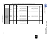


Table Of Contents
- Contents
- Preface
- Introduction
- 1.1 Introduction
- 1.2 EP93xx Features
- 1.3 EP93xx Processor Applications
- 1.4 EP93xx Processor Highlights
- 1.4.1 High-Performance ARM920T Core
- 1.4.2 MaverickCrunch™ Co-processor for Ultra-Fast Math Processing
- 1.4.3 MaverickKey™ Unique ID Secures Digital Content in OEM Designs
- 1.4.4 Integrated Multi-Port USB 2.0 Full Speed Hosts with Transceivers
- 1.4.5 Integrated Ethernet MAC Reduces BOM Costs
- 1.4.6 8x8 Keypad Interface Reduces BOM Costs
- 1.4.7 Multiple Booting Mechanisms Increase Flexibility
- 1.4.8 Abundant General Purpose I/Os Build Flexible Systems
- 1.4.9 General-Purpose Memory Interface (SDRAM, SRAM, ROM, FLASH)
- 1.4.10 12-Bit Analog-to-Digital Converter (ADC) Provides an Integrated Touch-Screen Interface or General ADC Functionality
- 1.4.11 Raster Analog / LCD Controller
- 1.4.12 Graphics Accelerator
- 1.4.13 PCMCIA Interface
- ARM920T Core and Advanced High-Speed Bus (AHB)
- MaverickCrunch Co-Processor
- 3.1 Introduction
- 3.2 Programming Examples
- 3.3 DSPSC Register
- 3.4 ARM Co-Processor Instruction Format
- 3.5 Instruction Set for the MaverickCrunch Co-Processor
- 3.5.1 Load and Store Instructions
- 3.5.2 Move Instructions
- 3.5.3 Accumulator and DSPSC Move Instructions
- 3.5.4 Copy and Conversion Instructions
- 3.5.5 Shift Instructions
- 3.5.6 Compare Instructions
- 3.5.7 Floating Point Arithmetic Instructions
- 3.5.8 Integer Arithmetic Instructions
- 3.5.9 Accumulator Arithmetic Instructions
- Boot ROM
- System Controller
- Vectored Interrupt Controller
- Raster Engine With Analog/LCD Integrated Timing and Interface
- 7.1 Introduction
- 7.2 Features
- 7.3 Raster Engine Features Overview
- 7.4 Functional Details
- 7.4.1 VILOSATI (Video Image Line Output Scanner and Transfer Interface)
- 7.4.2 Video FIFO
- 7.4.3 Video Pixel MUX
- 7.4.4 Blink Function
- 7.4.5 Color Look-Up-Tables
- 7.4.6 Color RGB Mux
- 7.4.7 Pixel Shift Logic
- 7.4.8 Grayscale/Color Generator for Monochrome/Passive Low Color Displays
- 7.4.9 Hardware Cursor
- 7.4.10 Video Timing
- 7.4.11 Blink Logic
- 7.4.12 Color Mode Definition
- 7.5 Registers
- Graphics Accelerator
- 1/10/100 Mbps Ethernet LAN Controller
- 9.1 Introduction
- 9.2 Descriptor Processor
- 9.2.1 Receive Descriptor Processor Queues
- 9.2.2 Receive Descriptor Queue
- 9.2.3 Receive Status Queue
- 9.2.3.1 Receive Status Format
- 9.2.3.2 Receive Flow
- 9.2.3.3 Receive Errors
- 9.2.3.4 Receive Descriptor Data/Status Flow
- 9.2.3.5 Receive Descriptor Example
- 9.2.3.6 Receive Frame Pre-Processing
- 9.2.3.7 Transmit Descriptor Processor Queues
- 9.2.3.8 Transmit Descriptor Queue
- 9.2.3.9 Transmit Descriptor Format
- 9.2.3.10 Transmit Status Queue
- 9.2.3.11 Transmit Status Format
- 9.2.3.12 Transmit Flow
- 9.2.3.13 Transmit Errors
- 9.2.3.14 Transmit Descriptor Data/Status Flow
- 9.2.4 Interrupts
- 9.2.5 Initialization
- 9.3 Registers
- DMA Controller
- 10.1 Introduction
- 10.1.1 DMA Features List
- 10.1.2 Managing Data Transfers Using a DMA Channel
- 10.1.3 DMA Operations
- 10.1.4 Internal M2P or P2M AHB Master Interface Functional Description
- 10.1.5 M2M AHB Master Interface Functional Description
- 10.1.6 AHB Slave Interface Limitations
- 10.1.7 Interrupt Interface
- 10.1.8 Internal M2P/P2M Data Unpacker/Packer Functional Description
- 10.1.9 Internal M2P/P2M DMA Functional Description
- 10.1.10 M2M DMA Functional Description
- 10.1.11 DMA Data Transfer Size Determination
- 10.1.12 Buffer Descriptors
- 10.1.13 Bus Arbitration
- 10.2 Registers
- 10.1 Introduction
- Universal Serial Bus Host Controller
- Static Memory Controller
- SDRAM, SyncROM, and SyncFLASH Controller
- UART1 With HDLC and Modem Control Signals
- UART2
- UART3 With HDLC Encoder
- IrDA
- Timers
- Watchdog Timer
- Real Time Clock With Software Trim
- I2S Controller
- AC’97 Controller
- Synchronous Serial Port
- 23.1 Introduction
- 23.2 Features
- 23.3 SSP Functionality
- 23.4 SSP Pin Multiplex
- 23.5 Configuring the SSP
- 23.5.1 Enabling SSP Operation
- 23.5.2 Master/Slave Mode
- 23.5.3 Serial Bit Rate Generation
- 23.5.4 Frame Format
- 23.5.5 Texas Instruments® Synchronous Serial Frame Format
- 23.5.6 Motorola® SPI Frame Format
- 23.5.7 Motorola SPI Format with SPO=0, SPH=0
- 23.5.8 Motorola SPI Format with SPO=0, SPH=1
- 23.5.9 Motorola SPI Format with SPO=1, SPH=0
- 23.5.10 Motorola SPI Format with SPO=1, SPH=1
- 23.5.11 National Semiconductor® Microwire™ Frame Format
- 23.6 Registers
- Pulse Width Modulator
- Analog Touch Screen Interface
- 25.1 Introduction
- 25.2 Touch Screen Controller Operation
- 25.2.1 Touch Screen Scanning: Four-wire and Eight-wire Operation
- 25.2.2 Five-wire and Seven-wire Operation
- 25.2.3 Direct Operation
- 25.2.4 Measuring Analog Input with the Touch Screen Controls Disabled
- 25.2.5 Measuring Touch Screen Resistance
- 25.2.6 Polled and Interrupt-Driven Modes
- 25.2.7 Touch Screen Package Dependency
- 25.3 Registers
- Keypad Interface
- IDE Interface
- GPIO Interface
- Security
- Glossary
- EP93XX Register List

DS785UM1 13-21
Copyright 2007 Cirrus Logic
SDRAM, SyncROM, and SyncFLASH Controller
EP93xx User’s Guide
1
3
1
3
13
Definition:
The Refresh Timer register is used to specify the period between refresh
cycles.
Bit Descriptions:
RSVD: Reserved. - Unknown During Read
Refcnt: Refresh Count - Read/Write
The value written to this field specifies, in multiples of the
period of HCLK, the time period between refresh cycles.
For example, if the period of HCLK is 20 ns, this field
should be written to 0x320 (decimal 800) to generate a
16 ms refresh period. On reset, this field defaults to
0x0080 (decimal 128) to generate a 2.56 ms refresh
period, but it must be written during the SDRAM
initialization routine to the appropriate value for the
SDRAM devices. If this field is written to 0x0000, no
refresh cycles are issued.
BootSts
Address: 0x8006_000C - Read Only
Default: 0x0000_0000
Definition:
When power on reset is asserted, the values of the boot mode option pins
shown in Table 13-1 are latched. The Boot Status register reflects those
latched values. This register can be read to determine which memory
configuration was used during the boot process.
Bit Descriptions:
RSVD: Reserved - Unknown During Read
ASDO: Latched ASDO pin value - Read Only
Boot Media:
1 - SyncROM or SyncFLASH
0 - Asynchronous ROM
Width: Boot memory bus Width - Read Only
31 30 29 28 27 26 25 24 23 22 21 20 19 18 17 16
RSVD
15 14 13 12 11 10 9 8 7 6 5 4 3 2 1 0
RSVD Latched
ASDO
Width