
Owner's manual
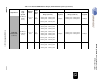


Table Of Contents
- Contents
- Preface
- Introduction
- 1.1 Introduction
- 1.2 EP93xx Features
- 1.3 EP93xx Processor Applications
- 1.4 EP93xx Processor Highlights
- 1.4.1 High-Performance ARM920T Core
- 1.4.2 MaverickCrunch™ Co-processor for Ultra-Fast Math Processing
- 1.4.3 MaverickKey™ Unique ID Secures Digital Content in OEM Designs
- 1.4.4 Integrated Multi-Port USB 2.0 Full Speed Hosts with Transceivers
- 1.4.5 Integrated Ethernet MAC Reduces BOM Costs
- 1.4.6 8x8 Keypad Interface Reduces BOM Costs
- 1.4.7 Multiple Booting Mechanisms Increase Flexibility
- 1.4.8 Abundant General Purpose I/Os Build Flexible Systems
- 1.4.9 General-Purpose Memory Interface (SDRAM, SRAM, ROM, FLASH)
- 1.4.10 12-Bit Analog-to-Digital Converter (ADC) Provides an Integrated Touch-Screen Interface or General ADC Functionality
- 1.4.11 Raster Analog / LCD Controller
- 1.4.12 Graphics Accelerator
- 1.4.13 PCMCIA Interface
- ARM920T Core and Advanced High-Speed Bus (AHB)
- MaverickCrunch Co-Processor
- 3.1 Introduction
- 3.2 Programming Examples
- 3.3 DSPSC Register
- 3.4 ARM Co-Processor Instruction Format
- 3.5 Instruction Set for the MaverickCrunch Co-Processor
- 3.5.1 Load and Store Instructions
- 3.5.2 Move Instructions
- 3.5.3 Accumulator and DSPSC Move Instructions
- 3.5.4 Copy and Conversion Instructions
- 3.5.5 Shift Instructions
- 3.5.6 Compare Instructions
- 3.5.7 Floating Point Arithmetic Instructions
- 3.5.8 Integer Arithmetic Instructions
- 3.5.9 Accumulator Arithmetic Instructions
- Boot ROM
- System Controller
- Vectored Interrupt Controller
- Raster Engine With Analog/LCD Integrated Timing and Interface
- 7.1 Introduction
- 7.2 Features
- 7.3 Raster Engine Features Overview
- 7.4 Functional Details
- 7.4.1 VILOSATI (Video Image Line Output Scanner and Transfer Interface)
- 7.4.2 Video FIFO
- 7.4.3 Video Pixel MUX
- 7.4.4 Blink Function
- 7.4.5 Color Look-Up-Tables
- 7.4.6 Color RGB Mux
- 7.4.7 Pixel Shift Logic
- 7.4.8 Grayscale/Color Generator for Monochrome/Passive Low Color Displays
- 7.4.9 Hardware Cursor
- 7.4.10 Video Timing
- 7.4.11 Blink Logic
- 7.4.12 Color Mode Definition
- 7.5 Registers
- Graphics Accelerator
- 1/10/100 Mbps Ethernet LAN Controller
- 9.1 Introduction
- 9.2 Descriptor Processor
- 9.2.1 Receive Descriptor Processor Queues
- 9.2.2 Receive Descriptor Queue
- 9.2.3 Receive Status Queue
- 9.2.3.1 Receive Status Format
- 9.2.3.2 Receive Flow
- 9.2.3.3 Receive Errors
- 9.2.3.4 Receive Descriptor Data/Status Flow
- 9.2.3.5 Receive Descriptor Example
- 9.2.3.6 Receive Frame Pre-Processing
- 9.2.3.7 Transmit Descriptor Processor Queues
- 9.2.3.8 Transmit Descriptor Queue
- 9.2.3.9 Transmit Descriptor Format
- 9.2.3.10 Transmit Status Queue
- 9.2.3.11 Transmit Status Format
- 9.2.3.12 Transmit Flow
- 9.2.3.13 Transmit Errors
- 9.2.3.14 Transmit Descriptor Data/Status Flow
- 9.2.4 Interrupts
- 9.2.5 Initialization
- 9.3 Registers
- DMA Controller
- 10.1 Introduction
- 10.1.1 DMA Features List
- 10.1.2 Managing Data Transfers Using a DMA Channel
- 10.1.3 DMA Operations
- 10.1.4 Internal M2P or P2M AHB Master Interface Functional Description
- 10.1.5 M2M AHB Master Interface Functional Description
- 10.1.6 AHB Slave Interface Limitations
- 10.1.7 Interrupt Interface
- 10.1.8 Internal M2P/P2M Data Unpacker/Packer Functional Description
- 10.1.9 Internal M2P/P2M DMA Functional Description
- 10.1.10 M2M DMA Functional Description
- 10.1.11 DMA Data Transfer Size Determination
- 10.1.12 Buffer Descriptors
- 10.1.13 Bus Arbitration
- 10.2 Registers
- 10.1 Introduction
- Universal Serial Bus Host Controller
- Static Memory Controller
- SDRAM, SyncROM, and SyncFLASH Controller
- UART1 With HDLC and Modem Control Signals
- UART2
- UART3 With HDLC Encoder
- IrDA
- Timers
- Watchdog Timer
- Real Time Clock With Software Trim
- I2S Controller
- AC’97 Controller
- Synchronous Serial Port
- 23.1 Introduction
- 23.2 Features
- 23.3 SSP Functionality
- 23.4 SSP Pin Multiplex
- 23.5 Configuring the SSP
- 23.5.1 Enabling SSP Operation
- 23.5.2 Master/Slave Mode
- 23.5.3 Serial Bit Rate Generation
- 23.5.4 Frame Format
- 23.5.5 Texas Instruments® Synchronous Serial Frame Format
- 23.5.6 Motorola® SPI Frame Format
- 23.5.7 Motorola SPI Format with SPO=0, SPH=0
- 23.5.8 Motorola SPI Format with SPO=0, SPH=1
- 23.5.9 Motorola SPI Format with SPO=1, SPH=0
- 23.5.10 Motorola SPI Format with SPO=1, SPH=1
- 23.5.11 National Semiconductor® Microwire™ Frame Format
- 23.6 Registers
- Pulse Width Modulator
- Analog Touch Screen Interface
- 25.1 Introduction
- 25.2 Touch Screen Controller Operation
- 25.2.1 Touch Screen Scanning: Four-wire and Eight-wire Operation
- 25.2.2 Five-wire and Seven-wire Operation
- 25.2.3 Direct Operation
- 25.2.4 Measuring Analog Input with the Touch Screen Controls Disabled
- 25.2.5 Measuring Touch Screen Resistance
- 25.2.6 Polled and Interrupt-Driven Modes
- 25.2.7 Touch Screen Package Dependency
- 25.3 Registers
- Keypad Interface
- IDE Interface
- GPIO Interface
- Security
- Glossary
- EP93XX Register List

DS785UM1 13-16
Copyright 2007 Cirrus Logic
SDRAM, SyncROM, and SyncFLASH Controller
EP93xx User’s Guide
1
3
1
3
13
Note: , the letter "N" represents four additional address bits used for chip select. See Table 13-12.
32-Bit Wide
Data Systems
(Continued)
0xN300_0000 - 0xN37F_FFFF
0xN400_0000 - 0xN47F_FFFF
0xN500_0000 - 0xN57F_FFFF
0xN600_0000 - 0xN67F_FFFF
512 Mbit (2 x
16-bit wide
device)
13 x 10 x
4 banks
128
Mbytes
0xN700_0000 - 0xN77F_FFFF
0xN800_0000 - 0xN87F_FFFF
0xN900_0000 - 0xN97F_FFFF
8 Mbytes 0xN000_0000 - 0xN7FF_FFFF
128
Mbytes
0xNA00_0000 - 0xNA7F_FFFF
0xNB00_0000 - 0xNB7F_FFFF
0xNC00_0000 - 0xNC7F_FFFF
0xND00_0000 - 0xND7F_FFFF
0xNE00_0000 - 0xNE7F_FFFF
0xNF00_0000 - 0xNF7F_FFFF
Table 13-11. EP93xx SDRAM Address Ranges (16-Bit Wide Data Systems) (Continued)
Organization
Device
Size,
Type
System
Address
Matrix
Total
Bank
Size
SROMLL = 0 SROMLL = 1
Continuous Address
Range (see Note)
Size of
Segment
Continuous Address
Range (see Note)
Size of
Segment