
Owner's manual


Table Of Contents
- Contents
- Preface
- Introduction
- 1.1 Introduction
- 1.2 EP93xx Features
- 1.3 EP93xx Processor Applications
- 1.4 EP93xx Processor Highlights
- 1.4.1 High-Performance ARM920T Core
- 1.4.2 MaverickCrunch™ Co-processor for Ultra-Fast Math Processing
- 1.4.3 MaverickKey™ Unique ID Secures Digital Content in OEM Designs
- 1.4.4 Integrated Multi-Port USB 2.0 Full Speed Hosts with Transceivers
- 1.4.5 Integrated Ethernet MAC Reduces BOM Costs
- 1.4.6 8x8 Keypad Interface Reduces BOM Costs
- 1.4.7 Multiple Booting Mechanisms Increase Flexibility
- 1.4.8 Abundant General Purpose I/Os Build Flexible Systems
- 1.4.9 General-Purpose Memory Interface (SDRAM, SRAM, ROM, FLASH)
- 1.4.10 12-Bit Analog-to-Digital Converter (ADC) Provides an Integrated Touch-Screen Interface or General ADC Functionality
- 1.4.11 Raster Analog / LCD Controller
- 1.4.12 Graphics Accelerator
- 1.4.13 PCMCIA Interface
- ARM920T Core and Advanced High-Speed Bus (AHB)
- MaverickCrunch Co-Processor
- 3.1 Introduction
- 3.2 Programming Examples
- 3.3 DSPSC Register
- 3.4 ARM Co-Processor Instruction Format
- 3.5 Instruction Set for the MaverickCrunch Co-Processor
- 3.5.1 Load and Store Instructions
- 3.5.2 Move Instructions
- 3.5.3 Accumulator and DSPSC Move Instructions
- 3.5.4 Copy and Conversion Instructions
- 3.5.5 Shift Instructions
- 3.5.6 Compare Instructions
- 3.5.7 Floating Point Arithmetic Instructions
- 3.5.8 Integer Arithmetic Instructions
- 3.5.9 Accumulator Arithmetic Instructions
- Boot ROM
- System Controller
- Vectored Interrupt Controller
- Raster Engine With Analog/LCD Integrated Timing and Interface
- 7.1 Introduction
- 7.2 Features
- 7.3 Raster Engine Features Overview
- 7.4 Functional Details
- 7.4.1 VILOSATI (Video Image Line Output Scanner and Transfer Interface)
- 7.4.2 Video FIFO
- 7.4.3 Video Pixel MUX
- 7.4.4 Blink Function
- 7.4.5 Color Look-Up-Tables
- 7.4.6 Color RGB Mux
- 7.4.7 Pixel Shift Logic
- 7.4.8 Grayscale/Color Generator for Monochrome/Passive Low Color Displays
- 7.4.9 Hardware Cursor
- 7.4.10 Video Timing
- 7.4.11 Blink Logic
- 7.4.12 Color Mode Definition
- 7.5 Registers
- Graphics Accelerator
- 1/10/100 Mbps Ethernet LAN Controller
- 9.1 Introduction
- 9.2 Descriptor Processor
- 9.2.1 Receive Descriptor Processor Queues
- 9.2.2 Receive Descriptor Queue
- 9.2.3 Receive Status Queue
- 9.2.3.1 Receive Status Format
- 9.2.3.2 Receive Flow
- 9.2.3.3 Receive Errors
- 9.2.3.4 Receive Descriptor Data/Status Flow
- 9.2.3.5 Receive Descriptor Example
- 9.2.3.6 Receive Frame Pre-Processing
- 9.2.3.7 Transmit Descriptor Processor Queues
- 9.2.3.8 Transmit Descriptor Queue
- 9.2.3.9 Transmit Descriptor Format
- 9.2.3.10 Transmit Status Queue
- 9.2.3.11 Transmit Status Format
- 9.2.3.12 Transmit Flow
- 9.2.3.13 Transmit Errors
- 9.2.3.14 Transmit Descriptor Data/Status Flow
- 9.2.4 Interrupts
- 9.2.5 Initialization
- 9.3 Registers
- DMA Controller
- 10.1 Introduction
- 10.1.1 DMA Features List
- 10.1.2 Managing Data Transfers Using a DMA Channel
- 10.1.3 DMA Operations
- 10.1.4 Internal M2P or P2M AHB Master Interface Functional Description
- 10.1.5 M2M AHB Master Interface Functional Description
- 10.1.6 AHB Slave Interface Limitations
- 10.1.7 Interrupt Interface
- 10.1.8 Internal M2P/P2M Data Unpacker/Packer Functional Description
- 10.1.9 Internal M2P/P2M DMA Functional Description
- 10.1.10 M2M DMA Functional Description
- 10.1.11 DMA Data Transfer Size Determination
- 10.1.12 Buffer Descriptors
- 10.1.13 Bus Arbitration
- 10.2 Registers
- 10.1 Introduction
- Universal Serial Bus Host Controller
- Static Memory Controller
- SDRAM, SyncROM, and SyncFLASH Controller
- UART1 With HDLC and Modem Control Signals
- UART2
- UART3 With HDLC Encoder
- IrDA
- Timers
- Watchdog Timer
- Real Time Clock With Software Trim
- I2S Controller
- AC’97 Controller
- Synchronous Serial Port
- 23.1 Introduction
- 23.2 Features
- 23.3 SSP Functionality
- 23.4 SSP Pin Multiplex
- 23.5 Configuring the SSP
- 23.5.1 Enabling SSP Operation
- 23.5.2 Master/Slave Mode
- 23.5.3 Serial Bit Rate Generation
- 23.5.4 Frame Format
- 23.5.5 Texas Instruments® Synchronous Serial Frame Format
- 23.5.6 Motorola® SPI Frame Format
- 23.5.7 Motorola SPI Format with SPO=0, SPH=0
- 23.5.8 Motorola SPI Format with SPO=0, SPH=1
- 23.5.9 Motorola SPI Format with SPO=1, SPH=0
- 23.5.10 Motorola SPI Format with SPO=1, SPH=1
- 23.5.11 National Semiconductor® Microwire™ Frame Format
- 23.6 Registers
- Pulse Width Modulator
- Analog Touch Screen Interface
- 25.1 Introduction
- 25.2 Touch Screen Controller Operation
- 25.2.1 Touch Screen Scanning: Four-wire and Eight-wire Operation
- 25.2.2 Five-wire and Seven-wire Operation
- 25.2.3 Direct Operation
- 25.2.4 Measuring Analog Input with the Touch Screen Controls Disabled
- 25.2.5 Measuring Touch Screen Resistance
- 25.2.6 Polled and Interrupt-Driven Modes
- 25.2.7 Touch Screen Package Dependency
- 25.3 Registers
- Keypad Interface
- IDE Interface
- GPIO Interface
- Security
- Glossary
- EP93XX Register List
7-18 DS785UM1
Copyright 2007 Cirrus Logic
Raster Engine With Analog/LCD Integrated Timing and Interface
EP93xx User’s Guide
7
7
7
Where FRAME[1:0] = FRAME_CNT3 or FRAME_CNT4 as defined by FRAME at address
Pixel_In,
VCNT[1:0] = VERT_CNT3 or VERT_CNT4 as defined by VERT at address Pixel_In, and
HCNT[1:0] = HORZ_CNT3 or HORZ_CNT4 as defined by HORZ at address Pixel_In.
This is the GrySclLUT table in an easily readable form. To understand how to use this table
and to know how to fill the table with correct values requires a good understanding on how
the table is used by the grayscale logic.
7.4.8.8 GrySclLUT Timing Diagram
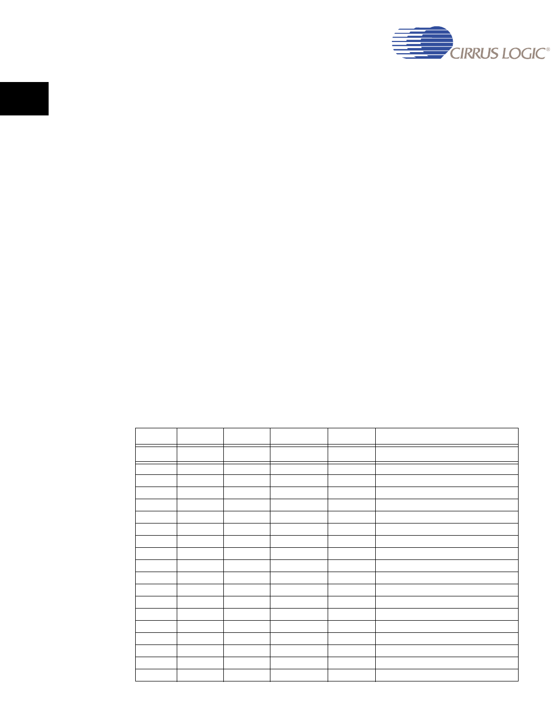
Table 7-5 shows the timing diagram. The clock column represents a free running master
clock for the display. This clock controls which pixel is being accessed as the image is being
rasterized on the display.
Assume that the first 8 registers have the HCNT, VCNT and FRAME counter registers set up
for 4 counts. The last column shows which register is used to retrieve the look up value and
the bit position within that register that is used as the source to send to the COLORMUX for
the given clock.
Clocks 4, 9, 14, and 19 represent all remaining pixels on the line. Clocks 24 and 29 represent
all remaining pixels for the frame. These entries will keep this example table to a manageable
size.
The FRAME count and PIXEL value are used to indicate which register contains the data.
HCNT and VCNT are used to indicate which bit in the identified register is to be used for the
given grayscale value.
Table 7-5. Grayscale Timing Diagram
Clock HCNT VCNT FRAME PIXEL Register Address / Value
Clock HCNT VCNT FRAME PIXEL Register Address / Value
0 0 0 0 5 (base + 94) / D0
1 1 0 0 5 (base + 94) / D1
2 2 0 0 5 (base + 94) / D2
3 3 0 0 5 (base + 94) / D3
4“ “ “ “
5 0 1 0 5 (base + 94) / D4
6 1 1 0 5 (base + 94) / D5
7 2 1 0 5 (base + 94) / D6
8 3 1 0 5 (base + 94) / D7
9“ “ “ “
10 0 2 0 5 (base + 94) / D8
11 1 2 0 5 (base + 94) / D9
12 2 2 0 5 (base + 94) / D10
13 3 2 0 5 (base + 94) / D11
14 “ “ “ “
15 0 3 0 5 (base + 94) / D12
16 1 3 0 5 (base + 94) / D13
17 2 3 0 5 (base + 94) / D14