
Manual


10 Copyright Cirrus Logic, Inc. 2011
(All Rights Reserved) DS507F2
EP7309
High-Performance, Low-Power System on Chip
Internal Boot ROM
The internal 128 byte Boot ROM facilitates download of saved
code to the on-board SRAM/FLASH.
Packaging
The EP7309 is available in a 208-pin LQFP package, 256-ball
PBGA package or a 204-ball TFBGA package.
Pin Multiplexing
The following table shows the pin multiplexing of the DAI,
SSI2 and the CODEC. The selection between SSI2 and the
CODEC is controlled by the state of the SERSEL bit in
SYSCON2. The choice between the SSI2, CODEC, and the
DAI is controlled by the DAISEL bit in SYSCON3 (see the
EP7309 User’s Manual for more information).
The following table shows the pins that have been multiplexed
in the EP7309.
Pin
Mnemonic
I/O DAI SSI2 CODEC
SSICLK I/O SCLK SSICLK PCMCLK
SSITXDA O SDOUT SSITXDA PCMOUT
SSIRXDA I SDIN SSIRXDA PCMIN
Table 17. DAI/SSI2/CODEC Pin Multiplexing
SSITXFR I/O LRCK SSITXFR PCMSYNC
SSIRXFR I MCLKIN SSIRXFR p/u
BUZ O MCLKOUT
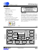
Signal Block Signal Block
RUN
System
Configuration
CLKEN
System
Configuration
nMEDCHG
Interrupt
Controller
nBROM
Boot ROM
select
PD[0] GPIO LEDFLSH LED Flasher
PE[1:0] GPIO BOOTSEL[1:0]
System
Configuration
PE[2] GPIO CLKSEL
System
Configuration
Table 18. Pin Multiplexing
Pin
Mnemonic
I/O DAI SSI2 CODEC
Table 17. DAI/SSI2/CODEC Pin Multiplexing