EP7309 Data Sheet FEATURES High-performance, Low-power, System-on-chip with Enhanced Digital Audio Interface ARM720T Processor — ARM7TDMI CPU — 8 KB of four-way set-associative cache — MMU with 64-entry TLB — Thumb code support enabled Ultra low power — 90 mW at 74 MHz typical — 30 mW at 18 MHz typical — 10 mW in the Idle State — <1 mW in the Standby State Advanced audio decoder/decompression capability — Supports bit streams with adaptive bit rates — Allows for support of multiple audio decompression alg
EP7309 High-Performance, Low-Power System on Chip FEATURES (cont) Dynamically programmable clock speeds of 18, 36, 49, and 74 MHz 48 KB of on-chip SRAM MaverickKey™ IDs — 32-bit unique ID can be used for SDMI compliance — 128-bit random ID LCD controller — Interfaces directly to a single-scan panel monochrome STN LCD — Interfaces to a single-scan panel color STN LCD with minimal external glue logic Full JTAG boundary scan and Embedded ICE support Integrated Peripheral Interfaces — 8/32/16-bit SRAM/FLASH/R
EP7309 High-Performance, Low-Power System on Chip Table of Contents FEATURES ..................................................................................................................................................................2 OVERVIEW ..................................................................................................................................................................2 Processor Core - ARM720T ........................................................................
EP7309 High-Performance, Low-Power System on Chip 256-Ball PBGA Ball Listing ........................................................................................................................ 30 JTAG Boundary Scan Signal Ordering ............................................................................................................... 34 CONVENTIONS .................................................................................................................................
EP7309 High-Performance, Low-Power System on Chip List of Figures Figure 1. A Maximum EP7309 Based System ..............................................................................................................11 Figure 2. Legend for Timing Diagrams .........................................................................................................................14 Figure 3. Static Memory Single Read Cycle Timing Measurement ......................................................................
EP7309 High-Performance, Low-Power System on Chip Processor Core - ARM720T The EP7309 incorporates an ARM 32-bit RISC microcontroller that controls a wide range of on-chip peripherals. The processor utilizes a three-stage pipeline consisting of fetch, decode and execute stages. Key features include: • • • • ARM (32-bit) and Thumb (16-bit compressed) instruction sets Enhanced MMU for Microsoft Windows CE and other operating systems 8 KB of 4-way set-associative cache.
EP7309 High-Performance, Low-Power System on Chip rates up to 115.2 kbps. An IrDA SIR protocol encoder/decoder can be optionally switched into the RX/TX signals to/from UART 1 to enable these signals to drive an infrared communication interface directly.
EP7309 High-Performance, Low-Power System on Chip Synchronous Serial Interface • • • ADC (SSI) Interface: Master mode only; SPI and Microwire1-compatible (128 kbps operation) Selectable serial clock polarity Pin Mnemonic I/O • • Pin Description ADCLK O SSI1 ADC serial clock ADCIN I SSI1 ADC serial input ADCOUT O SSI1 ADC serial output nADCCS O SSI1 ADC chip select SMPCLK O SSI1 ADC sample clock • • Column outputs can be individually set high with the remaining bits left at high-imped
EP7309 High-Performance, Low-Power System on Chip Pin Mnemonic Pin Description Pin Mnemonic Real-Time Clock Oscillator Input PA[7:0] I/O GPIO port A RTCOUT Real-Time Clock Oscillator Output PB[7:0] I/O GPIO port B VDDRTC Real-Time Clock Oscillator Power PD[0]/LEDFLSH I/O GPIO port D VSSRTC Real-Time Clock Oscillator Ground PD[5:1] I/O GPIO port D (Note) I/O GPIO port D PE[1:0]/BOOTSEL[1:0] (Note) I/O GPIO port E PE[2]/CLKSEL I/O GPIO port E PD[7:6]/SDQM[1:0] PLL and Clocking
EP7309 High-Performance, Low-Power System on Chip Internal Boot ROM The internal 128 byte Boot ROM facilitates download of saved code to the on-board SRAM/FLASH. Packaging The EP7309 is available in a 208-pin LQFP package, 256-ball PBGA package or a 204-ball TFBGA package. Pin Multiplexing The following table shows the pin multiplexing of the DAI, SSI2 and the CODEC. The selection between SSI2 and the CODEC is controlled by the state of the SERSEL bit in SYSCON2.
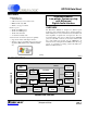
EP7309 High-Performance, Low-Power System on Chip System Design As shown in system block diagram, simply adding desired memory and peripherals to the highly integrated EP7309 CRYSTAL MOSCIN CRYSTAL RTCIN completes a low-power system solution. All necessary interface logic is integrated on-chip.
EP7309 High-Performance, Low-Power System on Chip ELECTRICAL SPECIFICATIONS Absolute Maximum Ratings DC Core, PLL, and RTC Supply Voltage 2.9 V DC I/O Supply Voltage (Pad Ring) 3.6 V DC Pad Input Current 10 mA/pin; 100 mA cumulative Storage Temperature, No Power –40C to +125C Recommended Operating Conditions DC core, PLL, and RTC Supply Voltage 2.5 V 0.2 V DC I/O Supply Voltage (Pad Ring) 2.3 V - 3.
EP7309 High-Performance, Low-Power System on Chip Symbol CI/O Parameter Transceiver capacitance IDDSTANDBY @ 25 C IDDSTANDBY @ 70 C IDDSTANDBY @ 85 C IDDidle at 74 MHz Standby current consumption1 Core, Osc, RTC @2.5 V I/O @ 3.3 V Standby current consumption1 Core, Osc, RTC @2.5 V I/O @ 3.3 V Min Typ Max Unit 8 - 10.0 pF - 77 41 - - - 570 111 µA Only nPOR, nPWRFAIL, nURESET, PE0, PE1, and RTS are driven, while all other float, VIH = VDD ± 0.1 V, VIL = GND ± 0.
EP7309 High-Performance, Low-Power System on Chip Timings Timing Diagram Conventions This data sheet contains timing diagrams. The following key explains the components used in these diagrams. Any variations are clearly labelled when they occur. Therefore, no additional meaning should be attached unless specifically stated.
EP7309 High-Performance, Low-Power System on Chip Static Memory Figure 3 through Figure 6 define the timings associated with all phases of the Static Memory. The following table contains the values for the timings of each of the Static Memory modes.
EP7309 High-Performance, Low-Power System on Chip Static Memory Single Read Cycle EXPCLK t CSd t CSh nCS t Ad A nM W E t M OEd t M OEh nM OE t HW d HALFW ORD t W Dd W ORD t Ds t Dh D t EXs t EXh EXPRDY t W Rd W RITE Figure 3. Static Memory Single Read Cycle Timing Measurement Note: 16 1. The cycle time can be extended by integer multiples of the clock period (22 ns at 45 MHz, 27 ns at 36 MHz, 54 ns at 18.
EP7309 High-Performance, Low-Power System on Chip Static Memory Single Write Cycle EXPCLK t CSd t CSh nCS t Ad A tM W d tM W h nM W E nM OE t HW d HALFW ORD t W Dd W ORD t Dv D t EXs t EXh EXPRDY W RITE Figure 4. Static Memory Single Write Cycle Timing Measurement Note: DS507F2 1. The cycle time can be extended by integer multiples of the clock period (22 ns at 45 MHz, 27 ns at 36 MHz, 54 ns at 18.
EP7309 High-Performance, Low-Power System on Chip Static Memory Burst Read Cycle EXPCLK t CSd t CSh nCS t Ad t Ah t Ah t Ah A nM W E t M OEd t M OEh nM OE t HW d HALF W ORD t W Dd W ORD t Ds t Dh t Ds t Dh t Ds t Dh t Ds t Dh D t EXs t EXh EXPRDY t W Rd W RITE Figure 5. Static Memory Burst Read Cycle Timing Measurement Note: 1. Four cycles are shown in the above diagram (minimum wait states, 1-0-0-0). This is the maximum number of consecutive cycles that can be driven.
EP7309 High-Performance, Low-Power System on Chip Static Memory Burst Write Cycle EXPCLK t CSd t CSh nCS t Ah t Ah t Ah t Ad A tM W d tM W d tM W d tM W h nM W E t MW d t MW h tM W h tM W h nM OE t HW d HALF W ORD W ORD t W Dd t Dv t Dnv t Dv t Dnv t Dv t Dnv t Dv D t EXs t EXh EXPRDY W RITE Figure 6. Static Memory Burst Write Cycle Timing Measurement Note: DS507F2 1. Four cycles are shown in the above diagram (minimum wait states, 1-1-1-1).
EP7309 High-Performance, Low-Power System on Chip SSI1 Interface Parameter Symbol Min Max Unit ADCCLK falling edge to nADCCSS deassert delay time tCd 9 10 ms ADCIN data setup to ADCCLK rising edge time tINs - 15 ns ADCIN data hold from ADCCLK rising edge time tINh - 14 ns ADCCLK falling edge to data valid delay time tOvd 7 13 ns ADCCLK falling edge to data invalid delay time tOd 2 3 ns ADC CLK tCd nADC CSS tINs tINh ADCIN tOvd tOd ADC OUT Figure 7.
EP7309 High-Performance, Low-Power System on Chip SSI2 Interface Parameter Symbol Min Max Unit SSICLK period (slave mode) tclk_per 185 2050 ns SSICLK high time tclk_high 925 1025 ns SSICLK low time tclk_low 925 1025 ns SSICLK rise/fall time tclkrf 3 18 ns SSICLK rising edge to RX and/or TX frame sync high time tFRd - 3 ns SSICLK rising edge to RX and/or TX frame sync low time tFRa - 8 ns tFR_per 960 990 ns SSIRXDA setup to SSICLK falling edge time tRXs 3 7 ns SSI
EP7309 High-Performance, Low-Power System on Chip LCD Interface Parameter Symbol Min Max Unit CL[2] falling to CL[1] rising delay time tCL1d 10 25 ns CL[1] falling to CL[2] rising delay time tCL2d 80 3,475 ns CL[1] falling to FRM transition time tFRMd 300 10,425 ns CL[1] falling to M transition time tMd 10 20 ns CL[2] rising to DD (display data) transition time tDDd 10 20 ns CL[2] t CL2d t CL1d CL[1] t FRM d FRM tM d M t DDd DD [3:0] Figure 9.
EP7309 High-Performance, Low-Power System on Chip JTAG Interface Parameter Symbol Min Max Units TCK clock period tclk_per 2 - ns TCK clock high time tclk_high 1 - ns TCK clock low time tclk_low 1 - ns JTAG port setup time tJPs - 0 ns JTAG port hold time tJPh - 3 ns JTAG port clock to output tJPco - 10 ns JTAG port high impedance to valid output tJPzx - 12 ns JTAG port valid output to high impedance tJPxz - 19 ns t clk_per t clk_high t clk_low TCK t JPh t JPs T
EP7309 High-Performance, Low-Power System on Chip Packages 208-Pin LQFP Package Characteristics 208-Pin LQFP Package Specifications 29.60 (1.165) 30.40 (1.197) 27.80 (1.094) 28.20 (1.110) 0.17 (0.007) 0.27 (0.011) 27.80 (1.094) 28.20 (1.110) EP7309 29.60 (1.165) 30.40 (1.197) 208-Pin LQFP 0.50 (0.0197) BSC Pin 1 Indicator Pin 208 Pin 1 1.35 (0.053) 1.45 (0.057) 0.45 (0.018) 0.75 (0.030) 1.00 (0.039) BSC 0.09 (0.004) 0.20 (0.008) 0 MIN 7 MAX 0.05 (0.002) 0.15 (0.006) 1.40 (0.055) 1.60 (0.
EP7309 High-Performance, Low-Power System on Chip 156 155 154 153 152 151 150 149 148 147 146 145 144 143 142 141 140 139 138 137 136 135 134 133 132 131 130 129 128 127 126 125 124 123 122 121 120 119 118 117 116 115 114 113 112 111 110 109 108 107 106 105 nURESET nMEDCHG/nBROM nPOR BATOK nEXTPWR nBATCHG D[7] VSSIO A[7] D[8] A[8] D[9] A[9] D[10] A[10] D[11] VSSIO VDDIO A[11] D[12] A[12] D[13] A[13] D[14] A[14] D[15] A[15] D[16] A[16] D[17] A[17] nTRST VSSIO VDDIO D[18] A[18 D[19] A[19] D[20] A[20] VSSIO
EP7309 High-Performance, Low-Power System on Chip 208-Pin LQFP Numeric Pin Listing Table 19. 208-Pin LQFP Numeric Pin Listing (Continued) Table 19. 208-Pin LQFP Numeric Pin Listing Pin No.
EP7309 High-Performance, Low-Power System on Chip Table 19. 208-Pin LQFP Numeric Pin Listing (Continued) Pin No. Signal Type Strength Reset State Pad Gnd 110 A[23] O 1 Low VDDIO Pad Pwr 111 D[23] I/O 1 Low DRIVE[1] I/O 112 A[22] O 1 Low Pin No.
EP7309 High-Performance, Low-Power System on Chip Table 19. 208-Pin LQFP Numeric Pin Listing (Continued) Table 19. 208-Pin LQFP Numeric Pin Listing (Continued) Pin No. Signal Type Strength Reset State Pin No.
EP7309 High-Performance, Low-Power System on Chip 256-Ball PBGA Package Characteristics 256-Ball PBGA Package Specifications 0.85 (0.034) ±0.05 (.002) 17.00 (0.669) ±0.20 (.008) Pin 1 Corner D1 0.40 (0.016) ±0.05 (.002) 15.00 (0.590) ±0.20 (.008) 30° TYP Pin 1 Indicator 17.00 (0.669) ±0.20 (.008) E1 15.00 (0.590) ±0.20 (.008) 2 Layer 0.36 (0.014) ±0.09 (0.004) TOP VIEW SIDE VIEW D 17.00 (0.669) Pin 1 Corner 1.00 (0.040) 1.00 (0.040) REF E 16 15 14 13 12 11 10 9 8 7 6 5 1.00 (0.
EP7309 High-Performance, Low-Power System on Chip 256-Ball PBGA Pinout (Top View)) 1 2 3 4 5 6 7 8 9 10 11 12 13 A VDDIO nCS[4] nCS[1] N/C N/C DD[1] M VDDIO D[0] D[2] A[3] VDDIO A[6] B nCS[5] VDDIO nCS[3] nMOE VDDIO N/C DD[2] CL[1] VDDCORE D[1] A[2] A[4] A[5] WAKEUP VDDIO nURESET B C VDDIO EXPCLK VSSIO VDDIO VSSIO VSSIO VSSIO VDDIO VSSIO VSSIO VSSIO VDDIO VSSIO VSSIO nPOR nEXTPWR C D WRITE EXPRDY VSSIO VDDIO nCS[2] nMWE N/C CL[2] VSSRTC
EP7309 High-Performance, Low-Power System on Chip Table 20. 256-Ball PBGA Ball Listing (Continued) Ball Location Name Type Description B7 DD[2] O LCD serial display data B8 CL[1] O LCD line clock B9 VDDCORE B10 D[1] I/O Data I/O Table 20. 256-Ball PBGA Ball Listing (Continued) Ball Location Core power Digital core power, 2.
EP7309 High-Performance, Low-Power System on Chip Table 20.
EP7309 High-Performance, Low-Power System on Chip Table 20.
EP7309 High-Performance, Low-Power System on Chip JTAG Boundary Scan Signal Ordering Table 21. JTAG Boundary Scan Signal Ordering 34 LQFP Pin No.
EP7309 High-Performance, Low-Power System on Chip Table 21. JTAG Boundary Scan Signal Ordering (Continued) DS507F2 LQFP Pin No.
EP7309 High-Performance, Low-Power System on Chip Table 21. JTAG Boundary Scan Signal Ordering (Continued) 36 LQFP Pin No.
EP7309 High-Performance, Low-Power System on Chip Table 21. JTAG Boundary Scan Signal Ordering (Continued) DS507F2 LQFP Pin No.
EP7309 High-Performance, Low-Power System on Chip Table 21. JTAG Boundary Scan Signal Ordering (Continued) LQFP Pin No. PBGA Ball Signal Type Position 201 D6 nMWE O 358 202 B4 nMOE O 360 204 E6 nCS[0] O 362 205 A3 nCS[1] O 364 206 D5 nCS[2] O 366 207 B3 nCS[3] O 368 208 A2 nCS[4] O 370 1) See EP7309 Users’ Manual for pin naming / functionality. 2) For each pad, the JTAG connection ordering is input, output, then enable as applicable.
EP7309 High-Performance, Low-Power System on Chip CONVENTIONS Table 22. Acronyms and Abbreviations (Continued) Acronym/ Abbreviation This section presents acronyms, abbreviations, units of measurement, and conventions used in this data sheet. Acronyms and Abbreviations Table 22 lists abbreviations and acronyms used in this data sheet. Table 22.
EP7309 High-Performance, Low-Power System on Chip General Conventions Pin Description Conventions Hexadecimal numbers are presented with all letters in uppercase and a lowercase “h” appended or with a 0x at the beginning. For example, 0x14 and 03CAh are hexadecimal numbers. Binary numbers are enclosed in single quotation marks when in text (for example, ‘11’ designates a binary number). Numbers not indicated by an “h”, 0x or quotation marks are decimal.
EP7309 High-Performance, Low-Power System on Chip Ordering Information Model Temperature EP7309-CBZ 0 to +70 °C EP7309-IBZ -40 to +85 °C EP7309-CVZ 0 to +70 °C EP7309-IVZ -40 to +85 °C Package 256-pin PBGA, 17mm X 17mm 208-pin LQFP. Environmental, Manufacturing, & Handling Information Model Number Peak Reflow Temp MSL Rating* Max Floor Life 260 °C 3 7 Days EP7309-CBZ EP7309-IBZ EP7309-CVZ EP7309-IVZ * MSL (Moisture Sensitivity Level) as specified by IPC/JEDEC J-STD-020.
EP7309 High-Performance, Low-Power System on Chip Revision History Revision Date Changes PP1 NOV 2003 First preliminary release. F1 AUG 2005 Updated ordering information. Added MSL data. F2 MAR 2011 Removed lead-containing device ordering information. Removed 204-pin BGA option. Contacting Cirrus Logic Support For all product questions and inquiries contact a Cirrus Logic Sales Representative. To find the one nearest to you go to www.cirrus.com IMPORTANT NOTICE Cirrus Logic, Inc.