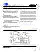
CS8952 CrystalLAN™ 100BASE-X and 10BASE-T Transceiver Features Description z Single-Chip IEEE 802.3 Physical Interface IC for The CS8952 uses CMOS technology to deliver a highperformance, low-cost 100BASE-X/10BASE-T Physical Layer (PHY) line interface. It makes use of an adaptive equalizer optimized for noise and near end crosstalk (NEXT) immunity to extend receiver operation to cable lengths exceeding 160 m.
CS8952 TABLE OF CONTENTS 1. SPECIFICATIONS AND CHARACTERISTICS......................................................... 3 2. INTRODUCTION ..................................................................................................... 18 2.1 High Performance Analog ............................................................................. 18 2.2 Low Power Consumption .............................................................................. 18 2.3 Application Flexibility.........................
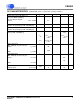
CS8952 1. SPECIFICATIONS AND CHARACTERISTICS ABSOLUTE MAXIMUM RATINGS (AVSS, DVSS = 0 V, all voltages with respect to 0 V.) Parameter Symbol VDD VDD_MII Power Supply Input Current Input Voltage Ambient Temperature Storage Temperature WARNING: Except Supply Pins Power Applied Min -0.3 -0.3 -0.3 -55 -65 Max 6.0 6.0 +/-10.0 VDD + 0.3 +125 +150 Unit V mA V °C °C Operation at or beyond these limits may result in permanent damage to the device. Normal operation is not guaranteed at these extremes.
CS8952 DC CHARACTERISTICS (Over recommended operating conditions) Parameter External Oscillator XTAL_I Input Low Voltage XTAL_I Input High Voltage XTAL_I Input Low Current XTAL_I Input High Current XTAL_I Input Capacitance XTAL_I Input Cycle Time XTAL_I Input Low Time XTAL_I Input High Time Power Supply Power Supply Current 100BASE-TX (Note 1) 100BASE-FX (Note 1) 10BASE-T (Note 1) Hardware Power-Down (Note 1) Software Power-Down (Note 1) Low Power Power-Up (Note 1) Digital I/O Output Low Voltage CLK25, M
CS8952 DC CHARACTERISTICS (CONTINUED) (Over recommended operating conditions) Parameter Output High Voltage (MII_DRV = 0) COL, CRS, MDIO, RXD[3:0], RX_CLK, RX_DV, RX_ER, TX_CLK IOH = -4.0mA Input Low Voltage All Inputs Except AN[1:0], TCM, TXSLEW[1:0] Input High Voltage All Inputs Except AN[1:0], TCM, TXSLEW[1:0] Tri-Level Input Voltages AN[1:0], TCM, TXSLEW[1:0] Input Low Current MDC, TXD[3:0], TX_CLK, TX_EN, TX_ER MDIO Min Typ Max 2.4 - - VIL - - 0.8 V VIH 2.
CS8952 10BASE-T CHARACTERISTICS Parameter 10BASE-T Interface Transmitter Differential Output Voltage (Peak) Receiver Normal Squelch Level (Peak) Receiver Low Squelch Level (LoRxSquelch bit set) 10BASE-T Transmitter TXD Pair Jitter into 100 Ω Load TXD Pair Return to ≤ 50 mV after Last Positive Transition TXD Pair Positive Hold Time at End of Packet 10BASE-T Receiver Allowable Received Jitter at Bit Cell Center Allowable Received Jitter at Bit Cell Boundary 10BASE-T Link Integrity First Transmitted Link Pulse
CS8952 100BASE-X CHARACTERISTICS Parameter 100BASE-TX Transmitter TX Differential Output Voltage (Peak) Signal Amplitude Symmetry Signal Rise/Fall Time Rise/Fall Symmetry Duty Cycle Distortion Overshoot/Undershoot Transmit Jitter TX Differential Output Impedance 100BASE-TX Receiver Receive Signal Detect Assert Threshold Receive Signal Detect De-assert Threshold Receive Signal Detect Assert Time Receive Signal Detect De-assert Time 100BASE-FX Transmitter TX_NRZ+/- Output Voltage - Low TX_NRZ+/- Output Voltag
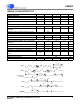
CS8952 100BASE-TX MII RECEIVE TIMING - 4B/5B ALIGNED MODES Parameter RX_CLK Period RX_CLK Pulse Width RXD[3:0],RX_ER/RXD4,RX_DV setup to rising edge of RX_CLK RXD[3:0],RX_ER/RXD4,RX_DV hold from rising edge of RX_CLK CRS to RXD latency 4B Aligned 5B Aligned “Start of Stream” to CRS asserted “End of Stream” to CRS de-asserted “Start of Stream” to COL asserted “End of Stream” to COL de-asserted RX_EN asserted to RX_DV, RXD[3:0] valid RX_EN de-asserted to RX_DV, RXD[3:0].
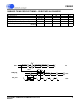
CS8952 100BASE-TX MII RECEIVE TIMING - 5B BYPASS ALIGN MODE Parameter RX_CLK Period RX_CLK Pulse Width RXD[4:0] setup to rising edge of RX_CLK RXD[4:0] hold after rising edge of RX_CLK Start of 5B symbol to symbol output on RX[4:0] 5B Mode RX+/- RX Symbol 0 Symbol tP tWL, tWH tSU tHD tRLAT RX Symbol N-1 tRLAT tSU RX Symbol N Typ 40 20 - Max 9 Unit ns ns ns ns BT IN tHD RX Data 0 RXD[4:0], Min 10 10 5 RX Data 1 OUT tP RX_CLK tWL tWH CrystalLAN™ 100BASE-X and 10BASE-T Transceiver DS206F1 O
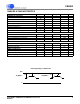
CS8952 100BASE-TX MII TRANSMIT TIMING - 4B/5B ALIGN MODES Parameter TXD[3:0] Setup to TX_CLK High TX_EN Setup to TX_CLK High TXD[3:0] Hold after TX_CLK High TX_ER Hold after TX_CLK High TX_EN Hold after TX_CLK High TX_EN “high” to CRS asserted latency TX_EN “low” to CRS de-asserted latency TX_EN “high” to TX+/- output (TX Latency) Symbol tSU1 tSU2 tHD1 tHD2 tHD3 tCRS1 Min 10 10 0 0 0 - tCRS2 - tLAT 6 Typ - 7 TX_CLK Unit ns ns ns ns ns BT 8 BT 8 BT Input/Output tSU2 tHD2 TX_EN Input tSU1 T
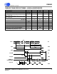
CS8952 100BASE-TX MII TRANSMIT TIMING - 5B BYPASS ALIGN MODE Parameter TXD[4:0] Setup to TX_CLK High TXD[4:0] Hold after TX_CLK High TX_ER Hold after TX_CLK High TXD[4:0] Sampled to TX+/- output (TX Latency) Symbol tSU1 tHD1 tHD2 tLAT TX_CLK Typ 6 Max 7 Unit ns ns ns ns Input/Output tSU1 TXD[4:0] Min 10 0 0 - tHD1 Data IN Input tLAT TX+/- Symbol OUT CrystalLAN™ 100BASE-X and 10BASE-T Transceiver DS206F1 Output 11
CS8952 10BASE-T MII RECEIVE TIMING Parameter RX_CLK Period RX_CLK Pulse Width RXD[3:0], RX_ER, RX_DV setup to rising edge of RX_CLK RXD[3:0], RX_ER, RX_DV hold from rising edge of RX_CLK RX data valid from CRS RX+/- preamble to CRS asserted RX+/- end of packet to CRS de-asserted RX+/- preamble to COL asserted RX+/- end of packet to COL de-asserted RX_EN asserted to RX_DV, RXD[3:0], RX_ER valid RX_EN de-asserted to RX_DV, RXD[3:0].
CS8952 10BASE-T MII TRANSMIT TIMING Parameter TXD[3:0] Setup to TX_CLK High TX_ER Setup to TX_CLK High TX_EN Setup to TX_CLK High TXD[3:0] Hold after TX_CLK High TX_ER Hold after TX_CLK High TX_EN Hold after TX_CLK High TX_EN “high” to CRS asserted latency TX_EN “low” to CRS de-asserted latency TX_EN “high” to TX+/- output (TX Latency) SQE Timing COL (SQE) Delay after CRS de-asserted COL (SQE) Pulse Duration Symbol tSU1 tSU2 tSU3 tHD1 tHD2 tHD3 tCRS1 tCRS2 tLAT Min 10 10 10 0 0 0 0 0 6 Typ - Max 4 16 14
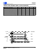
CS8952 10BASE-T SERIAL RECEIVE TIMING Parameter RX+/- active to RXD[0] active RX+/- active to CRS active RXD[0] setup from RX_CLK RXD[0] hold from RX_CLK RX_CLK hold after CRS off RXD[0] throughput delay CRS turn off delay Symbol tDATA tCRS tRDS tRDH tRCH tRD tCRSOFF Min 35 50 5 - Typ - Max 1200 600 250 400 Unit ns ns ns ns ns ns ns IN RX+/tCRSOFF tCRS tRD CRS tRCH OUT RX_CLK OUT tDATA tSU tHD RXD[0] CrystalLAN™ 100BASE-X and 10BASE-T Transceiver DS206F1 OUT 14
CS8952 10BASE-T SERIAL TRANSMIT TIMING Parameter TX_EN Setup from TX_CLK TX_EN Hold after TX_CLK TXD[0] Setup from TX_CLK TXD[0] Hold after TX_CLK Transmit start-up delay Transmit throughput delay Symbol tEHCH tCHEL tDSCH tCHDU tSTUD tTPD Min 10 10 10 10 - Typ - TX_CLK Unit ns ns ns ns ns ns Input/Output tEHCH tCHEL TX_EN Input tDSCH tCHDU Input TXD[0] tSTUD TX+/- Max 500 500 tPD Valid Data CrystalLAN™ 100BASE-X and 10BASE-T Transceiver DS206F1 Output 15
CS8952 AUTO NEGOTIATION / FAST LINK PULSE TIMING Parameter FLP burst to FLP burst FLP burst width Clock/Data pulses per burst Clock/Data pulse width Clock pulse to Data pulse Clock pulse to clock pulse Symbol tBTB tFLPW - tPW tCTD tCTC Min 15 17 55.5 111 Typ 16 2 100 64 128 Max 17 33 69.5 139 Unit ms ms ea.
CS8952 SERIAL MANAGEMENT INTERFACE TIMING Parameter Symbol tp tWL,tWH tMD1 tMD2 tMD3 MDC Period MDC Pulse Width MDIO Setup to MDC (MDIO as input) MDIO Hold after MDC (MDIO as input) MDC to MDIO valid (MDIO as output) Min 60 40 10 10 0 Typ - Max 60 40 Unit ns % ns ns ns DIRECTION: IN or OUT of chip MDC IN t MD1 t MD2 MDIO Valid Data Valid Data IN t MD3 MDIO Valid Data CrystalLAN™ 100BASE-X and 10BASE-T Transceiver DS206F1 OUT 17
CS8952 The CS8952 is a complete physical-layer transceiver for 100BASE-TX and 10BASE-T applications. Additionally, the CS8952 can be used with an external optical module for 100BASE-FX. to the Analog Design Considerations section for detailed information on power supply requirements and decoupling, crystal and magnetics requirements, and twisted-pair and fiber transceiver connections. 2.1 3. FUNCTIONAL DESCRIPTION 2.
CS8952 VDD_MII 4.99 kΩ 25 MHz 4.7 kΩ 0.1 µF 4.7 kΩ 1.5 kΩ XTAL_I XTAL_O 4 33 Ω 33 Ω RES VSS17 49.9 Ω 49.9 Ω RX+ TX_EN TX_CLK RX_CLK RXD[0] RXD[1]/PHYAD[1] RXD[2] RXD[3]/PHYAD[3] RX_ER/RXD[4]/PHYAD[4] RX_DV/MII_DRV COL/PHYAD0 CRS/PHYAD[2] 33 Ω 33 Ω 33 Ω 33 Ω 33 Ω 33 Ω 33 Ω 33 Ω MII I/F VSS18 MDIO MDC TXD TX_ER/TXD[4] RX- 75 Ω 51 Ω 51 Ω 51 Ω 75 Ω 51 Ω 51 Ω 51 Ω TX+ SHLD 8 7 6 5 RJ45 4 3 2 1 SHLD TX0.1 µF 0.1 µF 0.01 µF 2KV CS8952 VDD_MII 4.
CS8952 rupt signal to the controller when a change of state has occurred in the CS8952, eliminating the need for the system to poll the CS8952 for state changes. The RX_EN signal allows the receiver outputs to be electrically isolated. The ISODEF pin controls the value of register bit ISOLATE in the Basic Mode Control Register (address 00h) which in turn electrically isolates the CS8952's MII data path. 3.
CS8952 DATA and CONTROL Codes (RX_ER = 0 or TX_ER = 0) Name 5-bit Symbol 4-bit Nibble Comments 2 10100 0010 3 10101 0011 4 01010 0100 5 01011 0101 6 01110 0110 7 01111 0111 8 10010 1000 9 10011 1001 A 10110 1010 B 10111 1011 C 11010 1100 D 11011 1101 E 11100 1110 F 11101 1111 CONTROL (Note 2) I 11111 0101 IDLE (Note 3) J 11000 0101 First Start of Stream Symbol K 10001 0101 Second Start of Stream Symbol T 01101 0000 First End of Stream Symbol R 00111 0000 Second End of Stream Symbol 1.
CS8952 Code Violations (RX_ER = 1 or TX_ER = 1) Error Report Mode 4-bit Normal Mode 4-bit Nibble Comments Name 5-bit Symbol Nibble V6 01000 0110 or 0101 (Note 2) 1100 V7 01100 0110 or 0101 (Note 2) 1101 V8 10000 0110 or 0101 (Note 2) 1110 V9 11001 0110 or 0101 (Note 2) 1111 1. CONTROL code groups become violations when found in the data portion of the frame. 2.
CS8952 RX_CLK, RX_DV, COL, and CRS) onto a shared, external repeater system bus. 3.1.3 10BASE-T MII Application The digital interface used in this mode is the same as that used in the 100BASE-X MII mode except that TX_CLK and RX_CLK are nominally 2.5 MHz. The CS8952 includes a full-featured 10BASE-T interface, as described in the following sections. 3.1.3.
CS8952 Manchester Encoder and Decoder. Selection is made via: - setting bit 14 in the Basic Mode Control Register (address 00h) or - setting bits 8 and 11 in the Loopback, Bypass, and Receiver Error Mask Register (address 18h) or - asserting the LPBK pin. 3.1.3.7 Carrier Detection The carrier detect circuit informs the MAC that valid receive data is present by asserting the Carrier Sense signal (CRS) as soon it detects a valid bit pattern (1010b or 0101b for 10BASE-T).
CS8952 SET bit (bit 15 of the Basic Mode Control Register (address 00h)) is set. AN1 AN0 Low High Floating Floating Floating Low Low High High Floating Floating Low High Floating Low High Low High Forced/ Auto Forced Forced Forced Forced Auto-Neg Auto-Neg Auto-Neg Auto-Neg Auto-Neg Speed (Mb/s) 10 10 100 100 100/10 10 10 100 100 Full/Half Duplex Half Full Half Full Full/Half Half Full Half Full Table 5.
CS8952 STATUS Pins - COL - Collision indication, valid only for half duplex modes. - CRS - Carrier Sense indication SERIAL MANAGEMENT Pins - MDIO - a bi-directional serial data path - MDC - clock for MDIO (16.
CS8952 onto RXD[3:0] synchronously with respect to RX_CLK. presented to the CS8952. When TX_EN is not asserted, data on TXD[3:0] is ignored. Receive errors are indicated during frame reception by the assertion of RX_ER. It indicates that an error was detected somewhere in the frame currently being transferred across the MII. RX_ER will transition synchronously with respect to the RX_CLK, and will be held high for one cycle for each error received.
CS8952 TX_CLK TX_EN TXD[3:0] Preamble/SFD DATA TX_ER Figure 4. Transmission without errors TX_CLK TX_EN HALT TXD[3:0] Preamble/SFD DATA TX_ER Figure 5. Transmission with errors specification, while the remaining registers provide enhanced monitoring and control capabilities. As many as 31 devices may share a single Management Interface. A unique five-bit PHY address is associated with each device, with all devices responding to PHY address 00000.
CS8952 A read transaction is indicated by an Opcode of 10 and a write by 01. The PHY Address is five bits, with the most significant bit sent first. If the PHY address included in the frame is not 00000 or does not match the PHYAD field of the Self Status Register (address 19h), the rest of the frame is ignored. The register address is five bits, with the most significant bit sent first, and indicates the CS8952 register to be written to/read from.
CS8952 6. CS8952 REGISTERS The CS8952 register set is comprised of the 16-bit status and control registers described below. A detailed description each register follows.
CS8952 6.1 Basic Mode Control Register - Address 00h 15 Software Reset 14 Loopback 7 Collision Test BIT 15 14 6 NAME Software Reset Loopback 13 Speed Selection 12 Auto-Neg Enable 11 Power Down 10 Isolate 13 Speed Selection 12 Auto-Neg Enable 5 4 TYPE Read/Set RESET 0 Read/Write 0 11 10 Power Down Isolate 3 Reserved 2 9 Restart Auto-Neg 1 8 Duplex Mode 0 DESCRIPTION Setting this bit performs a chip-wide reset.
CS8952 9 BIT NAME Restart Auto-Neg TYPE Read/Set 8 Duplex Mode R/W 7 Collision Test R/W 6:0 Reserved Read Only RESET DESCRIPTION Setting this bit causes auto-negotiation to be restarted. It is an Act-Once bit which is cleared once auto-negotiation has begun. Clearing this bit has no effect on the auto-negotiation process. If auto-negotiation When bit 12 is clear, this bit controls the Fullis enabled via the Duplex/Half-Duplex operation of the part.
CS8952 6.
CS8952 3 BIT NAME Auto-Neg Ability TYPE Read Only 1 RESET 2 Link Status Read Only 0 1 Jabber Detect Read Only 0 DESCRIPTION This bit indicates that the CS8952 has auto-negotiation capability. Therefore this bit will always read back a value of 1. When set, this bit indicates that a valid link has been established. Upon a link failure, this bit is cleared and latched. It will remain cleared until this register is read.
CS8952 6.3 BIT 15:0 PHY Identifier, Part 1 - Address 02h 15 14 13 12 11 10 Organizationally Unique Identifier: Bits[3:10] 9 8 7 6 5 4 3 2 Organizationally Unique Identifier: Bits[11:18] 1 0 NAME Organizationally Unique Identifier (bits 3:18) TYPE RESET Read/Write 001Ah DESCRIPTION This identifier is assigned to PHY manufacturers by the IEEE. Its intention is to provide sufficient information to support 10/100 Management as defined in Clause 30.1.2 of the IEEE 802.3 specification.
CS8952 6.4 PHY Identifier, Part 2 - Address 03h 15 14 13 12 11 Organizationally Unique Identifier - Bits[19:24] 10 6 2 1 Revision Number 7 5 4 TYPE RESET Read/Write 00 1000 8 Part Number 3 Part Number BIT NAME 15:10 Organizationally Unique Identifier (bits 19:24) 9 0 DESCRIPTION This identifier is assigned to PHY manufacturers by the IEEE. Its intention is to provide sufficient information to support 10/100 Management as defined in Clause 30.1.2 of the IEEE 802.3 specification.
CS8952 6.
CS8952 6.
CS8952 6.
CS8952 6.
CS8952 6.9 Interrupt Mask Register - Address 10h 15 14 CIM Link Unstable Link Status Change 7 Reset Complete 6 Jabber Detect 13 12 Descrambler Premature End Lock Change Error 5 Auto-Neg Complete 4 Parallel Detection Fault 11 10 9 DCR Rollover FCCR Rollover RECR Rollover 3 Parallel Fail 2 Remote Fault 1 Page Received 8 Remote Loopback Fault 0 Reserved This register indicates which events will cause an interrupt event on the MII_IRQ pin. Each bit acts as an enable to the interrupt.
CS8952 BIT 11 10 9 8 7 6 NAME DCR Rollover FCCR Rollover RECR Rollover Remote Loopback Fault Reset Complete Jabber Detect TYPE Read/Write 0 RESET Read/Write 0 Read/Write 0 Read/Write 0 Read/Write 1 Read/Write 0 DESCRIPTION When set, an interrupt will be generated if the MSB in the DCR counter becomes set. Note: This bit is disabled, and writes to this bit are ignored when the National Compatibility Mode bit of the 10BASE-T Configuration Register (address 1Ch) is set.
CS8952 BIT 5 4 3 2 1 NAME TYPE Auto-Neg Complete Read/Write 0 Parallel Detection Fault Parallel Fail Remote Fault Page Received RESET Read/Write 0 Read/Write 0 Read/Write 0 Read/Write 0 DESCRIPTION When set, an interrupt will be generated once autonegotiation has completed successfully. Note: This bit is disabled, and writes to this bit are ignored when the National Compatibility Mode bit of the 10BASE-T Configuration Register (address 1Ch) is set.
CS8952 6.10 Interrupt Status Register - Address 11h 15 14 CIM Link Unstable Link Status Change 7 Reset Complete 6 Jabber Detect 13 12 Descrambler Premature End Lock Change Error 5 Auto-Neg Complete 4 Parallel Detection Fault 11 10 9 DCR Rollover FCCR Rollover RECR Rollover 3 Parallel Fail 2 Remote Fault 1 Page Received 8 Remote Loopback Fault 0 Reserved This register indicates which event(s) caused an interrupt event on the MII_IRQ pin.
CS8952 BIT 8 NAME Remote Loopback Fault TYPE Read Only RESET 0 7 Reset Complete Read Only 0 6 Jabber Detect Read Only 0 DESCRIPTION When set, this bit indicates that the Elastic Buffer has detected an over-run or an under-run condition. In any case, the frame generating this fault will be terminated.
CS8952 2 BIT NAME Remote Fault TYPE Read Only 0 RESET 1 Page Received Read Only 0 DESCRIPTION When auto-negotiation is enabled, this bit is set if the Remote Fault bit is set in the Auto-Negotiation Link Partner Ability Register (address 05h). When autonegotiation is disabled, this bit will be set when the Far-End Fault Indication for 100BASE-TX is detected. When set, this bit indicates that a valid word of autonegotiation data has been received and its integrity verified.
CS8952 6.11 BIT 15:0 Disconnect Count Register - Address 12h 15 14 13 12 11 Disconnect Counter 10 9 8 7 6 5 4 3 Disconnect Counter 2 1 0 NAME TYPE RESET Disconnect Counter Read/Write 0000h CrystalLAN™ 100BASE-X and 10BASE-T Transceiver DS206F1 DESCRIPTION This field contains a count of the number of times the CS8952 has lost a Link OK condition. This counter is cleared upon readout and will roll-over to 0000h.
CS8952 6.12 BIT 15:0 False Carrier Count Register - Address 13h 15 14 13 12 11 False Carrier Counter 10 9 8 7 6 5 4 3 False Carrier Counter 2 1 0 NAME False Carrier Counter TYPE Read Only RESET 0000h CrystalLAN™ 100BASE-X and 10BASE-T Transceiver DS206F1 DESCRIPTION This field contains a count of the number of times the CS8952 has detected a false-carrier -- that is, the reception of a poorly formed Start-of-Stream Delimiter (SSD).
CS8952 6.13 Scrambler Key Initialization Register - Address 14h 15 Load 14 7 6 BIT 15 13 12 11 10 Reserved NAME 5 TYPE Read/Set 4 3 Scrambler Initialization Key 2 9 8 Scrambler Initialization Key 1 0 RESET DESCRIPTION Load 0 When this bit is set, the scrambler will be loaded with the value in the Scrambler Initialization Key field. When the load is complete, this bit will clear automatically.
CS8952 6.14 BIT 15:0 Receive Error Count Register - Address 15h 15 14 13 12 11 Receive Error Counter 10 9 8 7 6 5 4 3 Receive Error Counter 2 1 0 NAME Receive Error Counter TYPE Read Only RESET 0000h CrystalLAN™ 100BASE-X and 10BASE-T Transceiver DS206F1 DESCRIPTION This counter increments for each packet in which one or more receive errors is detected that is not due to a collision event. This counter is cleared upon readout and will roll-over to 0000h.
CS8952 6.15 Descrambler Key Initialization Register - Address 16h 15 Load 14 7 6 BIT 15 13 12 11 Reserved NAME 5 TYPE Read/Set 4 3 Descrambler Initialization Key 10 9 8 Descrambler Initialization Key 2 1 0 RESET DESCRIPTION Load 0 When this bit is set, the descrambler will be loaded with the value in the Descrambler Initialization Key field. When the load is complete, this bit will clear automatically.
CS8952 6.
CS8952 BIT 9 8 NAME MF Preamble Enable Fast Test TYPE Read/Write 0 RESET Read/Write 0 7 CLK25 Disable Read/Write 6 Enable LT/100 Read/Write 5 CIM Disable Read/Write 4 Tx Disable Read/Write DESCRIPTION When set, this bit will force all management frames (via MDIO, MDC) to be preceded by a 32 bit preamble pattern of contiguous ones to be considered valid. When cleared, it allows management frames with or without the preamble pattern.
CS8952 BIT 3 NAME Rx Disable TYPE Read/Write 0 RESET DESCRIPTION When set, the receiver is disabled and no incoming packets pass through the receiver. The link will remain established and, if operating at 100 Mb/s, the descrambler will remain locked. When clear, the receiver is enabled. If Rx Disable is set while a packet is being received, reception is completed and no subsequent receive packets are allowed until Rx Disable is cleared again.
CS8952 6.
CS8952 BIT 8 7 NAME PMD Loopback Strip Preamble TYPE Read/Write 0 RESET Read/Write 0 6 Alternate FDX CRS Read/Write 0 5 Loopback Transmit Read/Write 1 Disable 4 Code Error Report Select Read/Write 0 DESCRIPTION When set, the scrambled NRZI transmit data is connected directly to the NRZI receive port on the descrambler. The loopback includes all of the 100BASE-TX functionality except for the MLT-3 encoding/decoding and the analog line-interface blocks.
CS8952 BIT 2 NAME Link Error Report Enable TYPE Read/Write 0 1 Packet Error Report Read/Write 0 Enable 0 Code Error Report Enable RESET Read/Write 0 DESCRIPTION When set, this bit causes link errors to be reported by a value of 3h on RXD[3:0] and the assertion of RX_ER. When clear, link errors are not reported across the MII. When set, this bit causes packet errors to be reported by a value of 2h on RXD[3:0] and the assertion of RX_ER. When clear, packet errors are not reported across the MII.
CS8952 6.
CS8952 BIT 5 4:0 NAME CIM Status TYPE Read Only RESET DESCRIPTION When clear, this bit indicates that a stable link connection has been detected. When an unstable link is detected and the Carrier Integrity Monitor Disable bit in the PCS Sub-Layer Configuration Register (address 17h) is clear, this bit is set and latched. It will remain set until this register is read. PHY Address Field Read/Write Reset to the val- The value on pins PHYAD[4:0] are latched into this field at power-up or reset.
CS8952 6.19 10BASE-T Status Register - Address 1Bh 15 14 13 12 11 Reserved 7 6 5 10 Polarity OK 4 3 2 9 10BASE-T Serial 1 8 Reserved 0 Reserved BIT NAME 15:11 Reserved 10 Polarity OK 9 10BASE-T Serial 8:0 Reserved TYPE Read Only Read Only RESET 0 0000 0 DESCRIPTION When high, the polarity of the receive signal (at the RXD+/RXD- inputs) is correct. If clear, the polarity is reversed.
CS8952 6.
CS8952 BIT 0 NAME Jabber Enable TYPE Read/Write 1 RESET DESCRIPTION When set, the jabber function is enabled. When clear, and if the CS8952 is in 10BASE-T full-duplex or 10BASE-T ENDEC loopback mode, the jabber function is disabled. Note: When the National Compatibility Mode bit (bit 7) is set, the Jabber function may also be disabled for 10BASE-T half-duplex, although this is not recommended. 7.
CS8952 +5 CS8952 SIGNALSIGNAL+ 68 Ω 82 Ω HFBR-5103 FIBER TRANS. 8 4 9 191 Ω 130 Ω +5 1 µH Ferrite Bead 5 +5 0.1 µF 0.1 µF 49.9 Ω TX_NRZTX_NRZ+ 63.4 Ω 49.9 Ω SD RxVCC 0.1 µF 1 µH Ferrite Bead 6 0.1 µF TxVCC 0.1 µF 4 7 5 8 TDTD+ +5 82 Ω RX_NRZRX_NRZ+ 82 Ω 6 3 7 2 130 Ω 1 130 Ω 9 RDRD+ RxVEE TxVEE Figure 7.
CS8952 with transformers meeting these requirements. However, the designer should evaluate the magnetics for suitability in their specific design. CS8952 VSS RES VSS 7.6 87 86 4.99 kΩ Via to Ground Plane 85 Figure 8. Biasing Resistor Connection and Layout plied through the XTAL_I pin, or using an external clock source supplied through the TX_CLK pin. When a 25 MHz crystal is used, it should be placed within one inch of the XTAL_I and XTAL_O pins of the CS8952.
CS8952 7.7 transmission lines (100 Ω differential, 50 Ω single-ended). The MII signals should be 68 Ω microstrip transmission lines. (For short MII signal paths one may standardize on a given trace width for all traces without significant degradation in signal integrity.) General Layout Recommendations The following PCB layout recommendations will help ensure reliable operation of the CS8952 and good EMC performance.
CS8952 ly) on both sides of the TX+/- traces. CS8952 Pin Assignment 91 (RX+) 92 (RX-) 81 (TX-) 80 (TX+) T1 Primary Pin T1 Secondary Assignment Pin Assignment 1 (RX+) 2 (RX-) 16 (TX-) 15 (TX+) 7 (RX+) 6 (RX-) 10 (TX-) 11 (TX+) RJ-45 Pin Assignment Adapter/NIC Configuration 3 (RD+) 6 (RD-) 2 (TD+) 1 (TD+) Hub/Repeater Configuration 1 (RD+) 2 (RD-) 6 (TD-) 3 (TD+) Table 8. RJ-45 Wiring • • No signal current carrying planes, i.e.
CS8952 8.
CS8952 MII Interface Pins COL/PHYAD0 - Collision Detect/PHY Address 0. Input/Tri-State Output, Pin 48. Asserted active-high to indicate a collision on the medium during half-duplex operation. In full-duplex operation, COL is undefined and should be ignored. When configured for 10 Mb/s operation, COL is also used to indicate a Signal Quality Error (SQE) condition. At power-up or at reset, the logic value on this pin is latched into bit 0 of the PHY Address field of the Self Status Register (address 19h).
CS8952 In order to conform with Annex 22B of the IEEE 802.3u specification, the MII_DRV pin should be pulled high during power-up or reset, and the RX_CLK pin should have an external 33 Ω series resistor. For systems not required to drive external connectors and cables as described in the IEEE802.3u specification, the external series resistor may not be necessary. RX_DV/MII_DRV - Receive Data Valid/MII Drive Strength. Input/Tri-State Output, Pin 33.
CS8952 RX_ER/PHYAD4/RXD4 - Receive Error/PHY Address 4/Receive Data 4. Input/Tri-State Output, Pin 37. During normal MII operation, this pin is defined as RX_ER (Receive Error). When RX_DV is high, RX_ER asserted high indicates that an error has been detected in the current receive frame. When RX_DV is low and RXD[3:0] = “1110”, RX_ER high indicates a False Carrier condition.
CS8952 When the TCM pin is high on power-up or reset, the CLK25 pin may be used as a source for the TX_CLK pin. When the TCM pin is floating on power-up or reset, TX_CLK must be supplied externally. TX_CLK should have the following nominal frequency: Speed 100 Mb/s 10 Mb/s 10 Mb/s 10BT_SER pin n/a low (parallel) high (serial) Nominal frequency 25 MHz 2.5 MHz 10 MHz TX_EN - Transmit Enable. Input, Pin 43. Asserted high to indicate valid data nibbles are present on TXD[3:0].
CS8952 AN1 pin 1 M M M 0 0 1 1 AN0 pin M 0 1 M 0 1 0 1 Speed 10 Mb/s 100 Mb/s 100 Mb/s 100/10 Mb/s 10 Mb/s 10 Mb/s 100 Mb/s 100 Mb/s Forced/Auto Forced Forced Forced Auto-Neg Auto-Neg Auto-Neg Auto-Neg Auto-Neg Full/Half Duplex Full Half Full Full/Half Half Full Half Full Auto-Negotiation may also be enabled and the advertised capabilities modified under software control through bit 8 of the Basic Mode Control Register (address 00h), and bits 5, 6, 7, 8, and 10 of the AutoNegotiation Advertisement Regi
CS8952 BP4B5B - Bypass 4B5B Coders. Input, Pin 56. When driven high during power-up or reset, the transmit 4B5B encoder and receiver 5B4B decoder are bypassed. Five-bit code groups are output and input on pins RXD[4:0] and TXD[4:0]. The 4B5B Coders may also be bypassed under software control through bit 14 of the Loopback, Bypass, and Receiver Error Mask Register (address 18h).
CS8952 ISODEF - Isolate Default. Input, Pin 63. When asserted high during power-up or reset, the MII will power-up electrically isolated except for the MDIO and MDC pins. When low, the part will exit reset fully electrically connected to the MII. The MII may also be isolated under software control through bit 10 of the Basic Mode Control Register (address 00h). At power-up or at reset, the value on this pin is latched into bit 10 of the Basic Mode Control Register (address 00h).
CS8952 LPSTRT - Low Power Start. Input, Pin 50. When this active-low input is asserted during power-up or reset, the CS8952 will exit reset in a low power configuration, where the only circuitry enabled is that necessary to maintain the media impedance. The CS8952 will remain in a low power state until RESET pin is asserted or the MDC pin toggles. This pin includes a weak internal pull-down (> 20 kΩ), or the value may be set by an external 4.7 kΩ pull-up or pull-down resistor. PWRDN - Power Down.
CS8952 REPEATER - REPEATER Mode Select. Input, Pin 16. This pin controls the operation of the CRS (Carrier Sense) pin as shown below: REPEATER pin high low low DUPLEX mode don’t care full duplex half duplex CRS Indicates receive activity only receive activity only receive or transmit activity At power-up or at reset, the value on this pin is latched into bit 12 of the PCS Sub-Layer Configuration Register (address 17h).
CS8952 TXSLEW[1:0] - Transmit Slew Rate Control. Input, Pins 61 and 60. These three-level pins allow adjustment to the rise and fall times of the 10BASE-TX transmitter output waveform. The rise and fall times are symmetric. TXSLEW0 pin low low low floating floating floating high high high TXSLEW1 mode low floating high low floating high low floating high Rise/Fall time 0.5 ns 1.0 ns 1.5 ns 2.0 ns 2.5 ns 3.0 ns 3.5 ns 4.0 ns 4.5 ns Media Interface Pins RX+, RX- - 10/100 Receive.
CS8952 RESET - Reset. Input, Pin 15. This active high input initializes the CS8952, and causes the CS8952 to latch the input signal on the following pins: COL/PHYAD0, CRS/PHYAD2, RX_ER/PHYAD4/RXD4, 10BT_SER, BP4B5B, BPALIGN, BPSCR, ISODEF, REPEATER, RXD[1]/PHYAD1, and RXD[3]/PHYAD3. XTAL_I - Crystal Input, Pin 96. XTAL_O - Crystal Output, Pin 97. A 25 MHz crystal should be connected across pins XTAL_I and XTAL_O.
CS8952 9. PACKAGE DIMENSIONS. 100L TQFP PACKAGE DRAWING E E1 D D1 1 e B ∝ A A1 L INCHES MIN MAX --0.063 0.002 0.006 0.007 0.011 0.618 0.642 0.547 0.555 0.618 0.642 0.547 0.555 0.016 0.024 0.018 0.030 0.000° 7.000° ∝ * Nominal pin pitch is 0.50 mm DIM A A1 B D D1 E E1 e* L MILLIMETERS MIN MAX --1.60 0.05 0.15 0.17 0.27 15.70 16.30 13.90 14.10 15.70 16.30 13.90 14.10 0.40 0.60 0.45 0.75 0.00° 7.00° Controlling dimension is mm.
CS8952 10. ORDERING INFORMATION Part # Temperature Range CS8952-CQZ 0 °C to +70 °C CS8952-IQZ -40 °C to +85 °C Package Description 100-lead TQFP, Lead (Pb) Free 11. ENVIRONMENTAL, MANUFACTURING, & HANDLING INFORMATION Model Number Peak Reflow Temp MSL Rating* Max Floor Life 260 °C 3 7 Days CS8952-CQZ CS8952-IQZ * MSL (Moisture Sensitivity Level) as specified by IPC/JEDEC J-STD-020.
CS8952 12. REVISION HISTORY Revision Date Changes PP3 OCT 2001 Initial Release. F1 JAN 2007 Added industrial temp range device. Added MSL data. Contacting Cirrus Logic Support For all product questions and inquiries contact a Cirrus Logic Sales Representative. To find one nearest you go to http://www.cirrus.com IMPORTANT NOTICE Cirrus Logic, Inc. and its subsidiaries ("Cirrus") believe that the information contained in this document is accurate and reliable.