
Instruction Manual

DS271F5 45
CS8900A
Crystal LAN™ Ethernet Controller
CIRRUS LOGIC PRODUCT DATASHEET
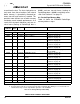
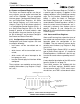
ing bus signals are tied to the following pins:
See Section 3.2 on page 18.
After reset, if no EEPROM is found by the CS8900A, then the register has the following initial state, which corre-
sponds to placing all the INTRQ pins in a high-impedance state. If an EEPROM is found, then the register's initial
value may be set by the EEPROM. See Section 3.3 on page 19.
Reset value is: XXXX XXXX XXXX X100
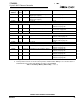
4.3.4 DMA Channel Number
(Read/Write, Address: PacketPage base + 0024h)
The DMA Channel register defines the DMA pins selected by the CS8900A. In the typical application, the following
bus signals are tied to the following pins:
See Section 3.2 on page 18 and Section 5.3 on page 90.
After reset, if no EEPROM is found by the CS8900A, then the register has the following initial state which corre-
sponds to setting all DMRQ pins to high-impedance. If a EEPROM is found, then the register's initial value may be
set by the EEPROM. See Section 3.3 on page 19.
Reset value is: XXXX XXXX XXXX XX11
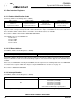
4.3.5 DMA Start of Frame
(Read only, Address: PacketPage base + 0026h)
The DMA Start of Frame Register contains a 16-bit value which defines the offset from the DMA base address to
the start of the most recently transferred received frame. See Section 5.3 on page 90.
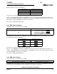
Bus signal Typical pin connection
IRQ5 INTRQ3
IRQ10 INTRQ0
IRQ11 INTRQ1
IRQ12 INTRQ2
Address 0025h Address 0024h
00h
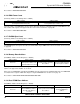
DMA channel assignment:
0000 0000b= pin DMRQ0 and DMACK0
0000 0001b= pin DMRQ1 and DMACK1
0000 0010b= pin DMRQ2 and DMACK2
0000 0011b= All DMRQ pins high-impedance
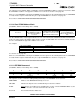
Bus signal Typical pin connection
DRQ5
DACK5
DMRQ0
DMACK0
DRQ6
DACK6
DMRQ1
DMACK1
DRQ7
DACK7
DMRQ2
DMACK2
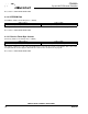
Address 0027h Address 0026h
Most significant byte of offset value Least significant byte of offset value