
Instruction Manual

108 DS271F5
CS8900A
Crystal LAN™ Ethernet Controller
CIRRUS LOGIC PRODUCT DATASHEET
6.2 Boundary Scan
Boundary Scan test mode provides an easy
and efficient board-level test for verifying that
the CS8900A has been installed properly.
Boundary Scan will check to see if the orienta-
tion of the chip is correct, and if there are any
open or short circuits.
Boundary Scan is controlled by the TEST pin.
When TEST is high, the CS8900A is config-
ured for normal operation. When TEST is low,
the following occurs:
• the CS8900A enters Boundary Scan test
mode and stays in this mode as long as
TEST is low;
• the CS8900A goes through an internal re-
set and remains in internal reset as long as
TEST is low;
• the AEN pin, normally the ISA bus Address
Enable, is redefined to become the Bound-
ary Scan shift clock input; and
• all digital outputs and bi-directional pins are
placed in a high-impedance state (this
electrically isolates the CS8900A digital
outputs from the rest of the circuit board).
For Boundary Scan to be enabled, AEN must
be low before TEST
is driven low.
A complete Boundary Scan test is made up of
two separate cycles. The first cycle, known as
the Output Cycle, tests all digital output pins
and all bi-directional pins. The second cycle,
known as the Input Cycle, tests all digital input
pins and all bi-directional pins.
6.2.1 Output Cycle
During the Output Cycle, the falling edge of
AEN causes each of the 17 digital output pins
and each of the 17 bi-directional pins to be
driven low, one at a time. The cycle begins
with LINKLED and advances in order counter-
clockwise around the chip through all 34 pins.
This test is referred to as a "walking 0" test.
The following is a list of output pins and bi-di-
rectional pins that are tested during the Output
Cycle:
The output pins not included in this test are:
6.2.2 Input Cycle
During the Input Cycle, the falling edge of AEN
causes the state of each selected pin to be
transferred to EEDataOut (that is, EEDataOut
will be high or low depending on the input level
of the selected pin). This cycle begins with
SLEEP and advances clockwise through each
of 33 input pins (all digital input pins except for
AEN) and each of the 17 bi-directional pins,
one pin at a time.
The following is a list of input pins and bi-direc-
tional pins that are tested during the Input Cy-
cle:
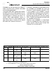
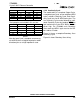
Pin Name Pin # Pin Name Pin #
ELCS 2 INTRQ1 31
EECS 3 INTRQ0 32
EESK 4 IOCS16 33
EEDataOut 5 MEMCS16 34
DMARQ2 11 INTRQ3 35
DMARQ1 13 IOCHRDY 64
DMARQ0 15 SD0 - SD7 65-68, 71-74
CSOUT 17 BSTATUS 78
SD08-SD15 27-24, 21-18 LINKLED 99
INTRQ2 30 LANLED 100
Table 39.
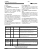
Pin Name Pin # Pin Name Pin #
DO+ 83 TXD- 88
DO- 84 RES 93
TXD+ 87 XTAL2 98
Table 40.
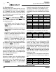
Pin Name Pin # Pin Name Pin #
ELCS 2 SBHE 36
EEDataIn 6 SA0 - SA11 37-48
CHIPSEL 7 REFRESH 49
DMACK2 12 SA12 - SA19 50-54, 58-60
Table 41.