
User Manual


CS8427
DS477F5 7
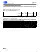
SWITCHING CHARACTERISTICS
Inputs: Logic 0 = 0 V, Logic 1 = VL+; C
L
= 20 pF.
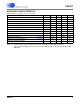
Notes: 6. Cycle-to-cycle locking to RXP/RXN using 32 to 96 kHz external PLL filter components.
7. PLL is bypassed (RXD1:0 bits in the Clock Source Control register set to 10b), clock is input to the
RMCK pin.
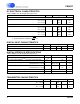
Parameter Symbol Min Typ Max Units
RST
pin Low Pulse Width 200 - - μs
OMCK Frequency for OMCK = 512 * Fso 4.1 - 55.3 MHz
OMCK Low and High Width for OMCK = 512 * Fso 7.2 - - ns
OMCK Frequency for OMCK = 384 * Fso 3.1 - 41.5 MHz
OMCK Low and High Width for OMCK = 384 * Fso 10.8 - - ns
OMCK Frequency for OMCK = 256 * Fso 2.0 - 27.7 MHz
OMCK Low and High Width for OMCK = 256 * Fso 14.4 - - ns
PLL Clock Recovery Sample Rate Range 8.0 - 108.0 kHz
RMCK output jitter (Note 6) - 200 - ps RMS
RMCK output duty cycle 40 50 60 %
RMCK Input Frequency (Note 7) 1.8 - 27.7 MHz
RMCK Input Low and High Width (Note 7) 14.4 - - ns
AES3 Transmitter Output Jitter - - 1 ns