
User Manual


CS8427
38 DS477F5
11.19 OMCK/RMCK Ratio (1Eh) (Read Only)
This register allows the calculation of the incoming sample rate by the host microcontroller from the
equation ORR=Fso/Fsi. The Fso is determined by OMCK, whose frequency is assumed to be
256xFso. ORR is represented as an unsigned 2-bit integer and a 6-bit fractional part. The value is
meaningful only after the PLL has reached lock. For example, if the OMCK is 12.288 MHz, Fso would
be 48 kHz (48 kHz = 12.288 MHz/256). Then if the input sample rate is also 48 KHz, you would get
1.0 from the ORR register. (The value from the ORR register is hexadecimal, so the actual value you
will get is 40h).
If F
SO
/F
SI
> 3.984375, ORR will overflow. Once the register has overflowed, the value shown will be
Fso/Fsi modulo 4. For example, if the OMCK is 36.864 MHz, Fso would be 144 kHz (144 kHz =
36.864 MHz/256). Then if the input sample rate is 32 kHz, you would get (144/32) mod 4 = 4.5 mod 4
= 0.5 from the ORR register. (The value from the ORR register is hexadecimal, so the actual value
you will get is 20h).
Also, there is no hysteresis on ORR. Therefore a small amount of jitter on either clock can cause the
LSB ORR[0] to oscillate.
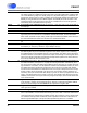
ORR[7:6] - Integer part of the ratio (Integer value=ORR[7:6])
ORR[5:0] - Fractional part of the ratio (Fraction value=ORR[5:0]/64)
11.20 C-bit or U-bit Data Buffer (20h - 37h)
Either channel status data buffer E or user data buffer E (provided UBM bits are set to block mode) is accessible
using these register addresses.
11.21 CS8427 I.D. and Version Register (7Fh) (Read Only)
ID3:0 - ID code for the CS8427. Permanently set to 0111
VER3:0 - CS8427 revision level. Revision A is coded as 0001
7 6 543210
ORR7 ORR6 ORR5 ORR4 ORR3 ORR2 ORR1 ORR0
7 6 543210
ID3 ID2 ID1 ID0 VER3 VER2 VER1 VER0