CS8427 96 kHz Digital Audio Interface Transceiver Features General Description Complete EIAJ CP1201, IEC-60958, AES3, S/PDIF-compatible Transceiver +5.0 V Analog Supply (VA+) +3.3 V or +5.
CS8427 TABLE OF CONTENTS 1. CHARACTERISTICS AND SPECIFICATIONS ......................................................................... 5 SPECIFIED OPERATING CONDITIONS ................................................................................. 5 ABSOLUTE MAXIMUM RATINGS ........................................................................................... 5 DC ELECTRICAL CHARACTERISTICS...................................................................................
CS8427 12. 13. 14. 15. 16. 17. 18. 19. 20. 21. DS477F5 11.14 Receiver Error (10h) (Read Only)................................................................................. 35 11.15 Receiver Error Mask (11h) ........................................................................................... 36 11.16 Channel Status Data Buffer Control (12h).................................................................... 36 11.17 User Data Buffer Control (13h) .............................................
CS8427 LIST OF FIGURES Figure 1. Audio Port Master Mode Timing....................................................................................... 8 Figure 2. Audio Port Slave Mode and Data Input Timing ................................................................ 8 Figure 3. SPI Mode timing............................................................................................................... 9 Figure 4. I²C Mode timing...........................................................................
CS8427 1. CHARACTERISTICS AND SPECIFICATIONS All Min/Max characteristics and specifications are guaranteed over the Specified Operating Conditions. Typical performance characteristics and specifications are derived from measurements taken at nominal supply voltages and TA = 25°C. SPECIFIED OPERATING CONDITIONS AGND, DGND = 0 V, all voltages with respect to 0 V.
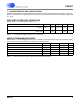
CS8427 DC ELECTRICAL CHARACTERISTICS AGND = DGND = 0 V; all voltages with respect to 0 V. Parameters Symbol Min Typ Max Units VA+ VL+ = 3.3 V VL+ = 5.0 V - 20 60 60 - μA μA μA Supply Current at 48 kHz frame rate VA+ VL+ = 3.3 V VL+ = 5.0 V - 6.3 30.1 46.5 - mA mA mA Supply Current at 96 kHz frame rate VA+ VL+ = 3.3 V VL+ = 5.0 V - 6.6 44.8 76.6 - mA mA mA Power-down Mode (Note 3) Supply Current in power down Normal Operation (Note 4) Notes: 3.
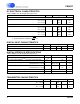
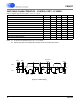
CS8427 SWITCHING CHARACTERISTICS Inputs: Logic 0 = 0 V, Logic 1 = VL+; CL = 20 pF. Parameter Symbol Min Typ Max Units RST pin Low Pulse Width 200 - - μs OMCK Frequency for OMCK = 512 * Fso 4.1 - 55.3 MHz OMCK Low and High Width for OMCK = 512 * Fso 7.2 - - ns OMCK Frequency for OMCK = 384 * Fso 3.1 - 41.5 MHz OMCK Low and High Width for OMCK = 384 * Fso 10.8 - - ns OMCK Frequency for OMCK = 256 * Fso 2.0 - 27.7 MHz OMCK Low and High Width for OMCK = 256 * Fso 14.
CS8427 SWITCHING CHARACTERISTICS - SERIAL AUDIO PORTS Inputs: Logic 0 = 0 V, Logic 1 = VL+; CL = 20 pF.
CS8427 SWITCHING CHARACTERISTICS - CONTROL PORT - SPI MODE Inputs: Logic 0 = 0 V, Logic 1 = VL+; CL = 20 pF. Parameter Symbol CCLK Clock Frequency (Note 14) Min Typ Max Units fsck 0 - 6.0 MHz CS High Time Between Transmissions tcsh 1.
CS8427 SWITCHING CHARACTERISTICS - CONTROL PORT - I²C MODE Note 17, Inputs: Logic 0 = 0 V, Logic 1 = VL+; CL = 20 pF. Parameter Symbol Min Typ Max Units SCL Clock Frequency fscl - - 100 kHz Bus Free Time Between Transmissions tbuf 4.7 - - μs Start Condition Hold Time (prior to first clock pulse) thdst 4.0 - - μs Clock Low Time tlow 4.7 - - μs Clock High Time thigh 4.0 - - μs Setup Time for Repeated Start Condition tsust 4.
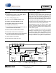
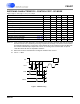
CS8427 2. TYPICAL CONNECTION DIAGRAM +5.0 V Analog Supply* Ferrite * Bead VA+ AES3/ SPDIF Source Cable Termination +3.3 V or +5.0 V Digital Supply 0.1μF 0.
CS8427 3. GENERAL DESCRIPTION The CS8427 is an AES3 transceiver intended to be used in digital audio systems. Such systems include digital mixing consoles, effects processors, digital recorders, and computer multimedia systems. 3.1 Audio Input/Output Ports The CS8427 has the following Audio ports: • Serial Audio Input Port • Serial Audio Output Port • AES3 or S/PDIF Receiver • AES3 or S/PDIF Transmitter The Serial Audio ports use a three-wire format.
CS8427 SPD1-0 ILRCK ISCLK SDIN Serial Audio Input Serial Audio Output OLRCK OSCLK SDOUT AESBP TXOFF RXN RXP AES3 Receiver TXP AES3 Encoder TXN TXD1-0 Channel Status and User Data Recovery SDA/CDOUT SCL/CCLK AD2/EMPH AD1/CDIN AD0/CS INT Channel Status Bits D E F User Bits D E F Control Port Control Registers Output Clock Generator OMCK Figure 6. CS8427 Internal Block Diagram Channel Status bits.
CS8427 clock routing and the associated control register bits. The clock routing constraints determine which data routing options are actually usable. Users should note that not all the possible data flow switch setting combinations are valid, because of the clock distribution architecture. The AESBP switch, shown in Figure 7, allows a TTL level bi-phase, mark-encoded data stream connected to RXP to be routed to the TXP and TXN pin drivers.
CS8427 5. THREE-WIRE SERIAL AUDIO PORTS A 3-wire serial audio input port and a 3-wire serial audio output port is provided. Each port can be adjusted to suit the attached device by setting the control registers. The following parameters are adjustable: master or slave, serial clock frequency, audio data resolution, left or right justification of the data relative to left/right clock, optional 1-bit cell delay of the 1st data bit, the polarity of the bit clock, and the polarity of the left/right clock.
CS8427 6. AES3 RECEIVER 6.3 The CS8427 includes an AES3 digital audio receiver and an AES3 digital audio transmitter. A comprehensive buffering scheme provides read/write access to the channel status and user data. This buffering scheme is described in “Appendix B: Channel Status and User Data Buffer Management”. While decoding the incoming AES3 data stream, the CS8427 can identify several kinds of error, indicated in the Receiver Error register.
CS8427 General on the incoming AES3 stream, copyright will always be indicated even when the stream indicates no copyright. Finally, the AUDIO bit is extracted and used to set an AUDIO indicator, as described in the Non-Audio Auto-Detection section below. If the incoming user data bits have been encoded as Q-channel subcode, the data is decoded and presented in ten consecutive register locations.
CS8427 7. AES3 TRANSMITTER The AES3 transmitter encodes and transmits audio and digital data according to the AES3, IEC60958 (S/PDIF), and EIAJ CP-1201 interface standards. Audio and control data are multiplexed together and bi-phase, mark encoded. The resulting bit stream is driven to an output connector either directly or through a transformer. The transmitter clock may be derived from the clock input pin OMCK, or from the incoming data.
CS8427 8. MONO MODE OPERATION An AES3 stream may be used in more than one way to transmit 96-kHz sample rate data. One method is to double the frame rate of the current format. This results in a stereo signal with a sample rate of 96 kHz, carried over a single twisted pair cable. An alternate method is implemented using the two sub-frames in a 48-kHz frame rate AES3 signal to carry consecutive samples of a mono signal, resulting in a 96-kHz sample rate stream.
CS8427 SDIN ISCLK SIMS SERIAL AUDIO INPUT ILRCK RXD0 RMCKF 1 MUX 0 ÷ PLL MUX RXP 0 SDOUT OUTPUT OLRCK OSCLK INC TXN CHANNEL AES3 STATUS TRANSMIT MEMORY 1 SERIAL AUDIO TXP USER 1 0 MUX BIT SWCLK UNLOCK MEMORY 1 0 MUX OUTC 0 MUX RMCK ÷ 1 RXD1 * OMCK CLK[1:0] Note: When SWCLK mode is enabled, signal input on OMCK is only output through RMCK and not routed back through the RXD1 multiplexer; RMCK is not bi-directional in this mode. Figure 8.
CS8427 SDOUT OSCLK OLRCK SDIN ISCLK ILRCK Serial Serial Audio Audio Output Input AES3 Rx & Decode RXN RXP RXN AES3 Encoder & Driver TXP RXP TXN AES3 Rx & Decode Serial Audio Output OLRCK OSCLK SDOUT PLL PLL RMCK Data Flow Control Bits TXD1-0: 01 SPD1-0: 10 RMCK Clock Source Control Bits OUTC: 1 INC: 0 RXD1-0: 01 Figure 9.
CS8427 VLRCK U (Out) VLRCK is a virtual word clock, which may not exist, but is used to illustrate the U timing. VLRCK duty cycle is 50%. VLRCK frequency is always equal to the incoming frame rate. If the serial audio output port is in master mode, VLRCK = OLRCK. If the serial audio output port is in slave mode, then VLRCK needs to be externally created, if required. U transitions are aligned within ±1% of VLRCK period to VLRCK edges Figure 13.
CS8427 Left Justified (In) ILRCK Channel A ISCLK SDIN MSB LSB ILRCK I²S (In) Channel B MSB LSB Channel A MSB Channel B ISCLK SDIN Right Justified (In) MSB MSB LSB ILRCK Channel A MSB LSB Channel B ISCLK SDIN MSB LSB MSB LSB SIMS* SISF* SIRES*[1:0] SIJUST* SIDEL* SISPOL* SILRPOL* Left Justified X X 00+ 0 0 0 0 I²S X X 00+ 0 1 0 1 Right Justified X X XX 1 0 0 0 X = don’t care to match format, but does need to be set to the desired setting + I²S can a
CS8427 OLRCK Left Justified OSCLK (Out) SDOUT Channel A LSB MSB OLRCK I²S (Out) MSB LSB Channel A MSB Channel B OSCLK SDOUT LSB MSB OLRCK Right Justified OSCLK (Out) SDOUT AES3 Direct (Out) Channel B MSB Channel A MSB Extended OLRCK Channel B LSB MSB MSB Extended Channel B Channel A MSB LSB MSB LSB Channel A Channel B OSCLK SDOUT LSB MSB V U C LSB MSB V U C Z LSB MSB V U C Z LSB SODEL* SOSPOL* SOLRPOL* MSB V U C Frame 0 Frame 191 SOMS* SOSF* SORES[1:0]* SOJUST
CS8427 9. CONTROL PORT DESCRIPTION AND TIMING The control port is used to access the registers, allowing the CS8427 to be configured for the desired operational modes and formats. In addition, Channel Status and User data may be read and written through the control port. The operation of the control port may be completely asynchronous with respect to the audio sample rates. However, to avoid potential interference problems, the control port pins should remain static if no operation is required.
CS8427 bits. In addition, each source may be set to rising edge, falling edge, or level-sensitive. Combined with the option of level-sensitive or edge-sensitive modes within the microcontroller, many different set-ups are possible depending on the needs of the equipment designer. mode is used for active-low, wired-OR hook-ups with multiple peripherals connected to the microcontroller interrupt input pin. Many conditions can cause an interrupt, as listed in the interrupt status register descriptions.
CS8427 10.
CS8427 11. CONTROL PORT REGISTER BIT DEFINITIONS 11.
CS8427 MMR - Select AES3 receiver mono or stereo operation Default = ‘0’ 0 - Normal stereo operation 1 - A and B subframes treated as consecutive samples of one channel of data. Data is duplicated to both left and right parallel outputs of the AES receiver block.
CS8427 SPD1:SPD0 - Serial Audio Output Port Data Source Default = ‘10’ 00 - Reserved 01 - Serial Audio Input Port 10 - AES3 receiver 11 - Reserved 11.4 Clock Source Control (04h) 7 6 5 4 3 2 1 0 0 RUN CLK1 CLK0 OUTC INC RXD1 RXD0 This register configures the clock sources of various blocks. In conjunction with the Data Flow Control register, various Receiver/Transmitter/Transceiver modes may be selected.
CS8427 11.
CS8427 SORES1:0 - Resolution of the output data on SDOUT and on the AES3 output Default = ‘00’ 00 - 24-bit resolution 01 - 20-bit resolution 10 - 16-bit resolution 11 - Direct copy of the received NRZ data from the AES3 receiver (including C, U, and V bits, the time slot normally occupied by the P bit is used to indicate the location of the block start, SDOUT pin only, serial audio output port clock must be derived from the AES3 receiver recovered clock) SOJUST - Justification of SDOUT data relative to OLRC
CS8427 11.8 Interrupt 2 Status (08h) (Read Only) 7 6 5 4 3 2 1 0 0 0 0 0 DETU EFTU QCH 0 For all bits in this register, a “1” means the associated interrupt condition has occurred at least once since the register was last read. A ”0” means the associated interrupt condition has NOT occurred since the last reading of the register. Reading the register resets all bits to 0, unless the interrupt mode is set to level and the interrupt source is still true.
CS8427 11.11 Interrupt 2 Mask (0Ch) 7 6 5 4 3 2 1 0 0 0 0 0 DETUM EFTUM QCHM 0 The bits of this register serve as a mask for the Interrupt 2 register. If a mask bit is set to 1, the error is unmasked, meaning that its occurrence will affect the INT pin and the status register. If a mask bit is set to 0, the error is masked, meaning that its occurrence will not affect the INT pin or the status register. The bit positions align with the corresponding bits in the Interrupt 2 register.
CS8427 AUDIO - Audio indicator 0 - Received data is linearly coded PCM audio 1 - Received data is not linearly coded PCM audio COPY - SCMS copyright indicator 0 - Copyright asserted 1 - Copyright not asserted If the category code is set to General in the incoming AES3 stream, copyright will always be indicated by COPY, even when the stream indicates no copyright. ORIG - SCMS generation indicator, decoded from the category code and the L bit.
CS8427 11.15 Receiver Error Mask (11h) 7 6 5 4 3 2 1 0 0 QCRCM CCRCM UNLOCKM VM CONFM BIPM PARM The bits in this register serve as masks for the corresponding bits of the Receiver Error register. If a mask bit is set to 1, the error is unmasked, meaning that its occurrence will appear in the receiver error register, will affect the RERR pin, will affect the RERR interrupt, and will affect the current audio sample according to the status of the HOLD bit.
CS8427 11.17 User Data Buffer Control (13h) 7 6 5 4 3 2 1 0 0 0 0 UD UBM1 UBM0 DETUI EFTUI UD - User data pin (U) direction specifier If this bit is changed during normal operation, then always stop the CS8427 first (RUN = 0), write the new value, then start the CS8427 (RUN = 1). Default = ‘0’ 0 - The U pin is an input. The U data is latched in on both rising and falling edges of OLRCK. This setting also chooses the U pin as the source for transmitted U data. 1 - The U pin is an output.
CS8427 11.19 OMCK/RMCK Ratio (1Eh) (Read Only) 7 6 5 4 3 2 1 0 ORR7 ORR6 ORR5 ORR4 ORR3 ORR2 ORR1 ORR0 This register allows the calculation of the incoming sample rate by the host microcontroller from the equation ORR=Fso/Fsi. The Fso is determined by OMCK, whose frequency is assumed to be 256xFso. ORR is represented as an unsigned 2-bit integer and a 6-bit fractional part. The value is meaningful only after the PLL has reached lock. For example, if the OMCK is 12.
CS8427 12. PIN DESCRIPTION - SOFTWARE MODE SDA/CDOUT AD0/CS EMPH RXP RXN VA+ AGND FILT RST RMCK RERR ILRCK ISCLK SDIN 1 2 3+ 4* 5* 6* 7* 8* 9* 10* 11* 12* 13* 14* 28 27 *26 *25 *24 *23 *22 21 20 19 *18 *17 *16 *15 SCL/CCLK AD1/CDIN TXP TXN H/S VL + DGND OMCK U INT SDOUT OLRCK OSCLK TCBL * Pins which remain the same function in all modes. + Pins which require a pull up or pull down resistor to select the desired startup option.
CS8427 RERR 11 Receiver Error (Output) - When high, indicates an error condition from the AES3 receiver. The status of this pin is updated once per sub-frame of incoming AES3 data. Conditions that can cause RERR to go high are: validity, parity error, bi-phase coding error, confidence, as well as loss of lock by the PLL. Each condition may be optionally masked from affecting the RERR pin using the Receiver Error Mask Register.
CS8427 TXP TXN 25 26 Differential Line Driver (Output) - Drivers transmit AES3 data and are pulled low while the CS8427 is in the reset state. AD1/CDIN 27 Address Bit 1 (I²C) / Serial Control Data in (SPI) (Input) - In I²C mode, AD1 is a chip address pin. In SPI mode, CDIN is the input data line for the control port interface SCL/CCLK 28 Control Port Clock (Input) - Serial control interface clock and is used to clock control data bits into and out of the CS8427.
CS8427 13. HARDWARE MODE DESCRIPTION Hardware mode is selected by connecting the H/S pin to ‘1’. Hardware Mode data flow is shown in Figure 19. Audio data is input through the AES3 receiver, and routed to the serial audio output port. Different audio data synchronous to RMCK may be input into the serial audio input port, and output through the AES3 transmitter.
CS8427 SDOUT RMCK RERR ORIG COPY LO - - - - Serial Output Port is Slave Function HI - - - - Serial Output Port is Master - - - - LO Mode A: C transmitted data is copied from received data, U and V =0, received PRO, EMPH, AUDIO is visible - - - - HI Mode B: CUV transmitted data is input serially on pins, received PRO, EMPH and AUDIO is not visible - LO LO - - Serial Input & Output Format: Left Justified - LO HI - - Serial Input & Output Format: I²S - HI LO - - S
CS8427 14. PIN DESCRIPTION - HARDWARE MODE COPY DGND2 EMPH/U RXP RXN VA+ AGND FILT RST RMCK RERR ILRCK ISCLK SDIN 1+ 2 3 4* 5* 6* 7* 8* 9* 10*+ 11*+ 12* 13* 14* +28 27 *26 *25 *24 *23 *22 21 20 19 +*18 *17 *16 *15 ORIG VL 2+ TXP TXN H/S VL + DGND APMS PRO/C AUDIO/V SDOUT OLRCK OSCLK TCBL * Pins which remain the same function in all modes. + Pins which require a pull up or pull down resistor to select the desired startup option.
CS8427 ILRCK 12 Serial Audio Input Left/Right Clock (Input/Output) - Word rate clock for the audio data on the SDIN pin. ISCLK 13 Serial Audio Bit Clock (Input/Output) - Serial bit clock for audio data on the SDIN pin. SDIN 14 Serial Audio Data Port (Input) - Audio data serial input pin. TCBL 15 Transmit Channel Status Block Start (Input/Output) - When operated as output, TCBL is high during the first sub-frame of a transmitted channel status block, and low at all other times.
CS8427 15. APPLICATIONS 15.1 Reset, Power Down and Start-up When RST is low, the CS8427 enters a low power mode and all internal states are reset, including the control port and registers, and the outputs are muted. When RST is high, the control port becomes operational and the desired settings should be loaded into the control registers. Writing a 1 to the RUN bit will then cause the part to leave the low power state and begin operation.
CS8427 16. PACKAGE DIMENSIONS 28L SOIC (300 MIL BODY) PACKAGE DRAWING E H 1 b c ∝ D L SEATING PLANE A e DIM A A1 b C D E e H L ∝ A1 MIN 0.093 0.004 0.013 0.009 0.697 0.291 0.040 0.394 0.016 0° INCHES NOM 0.098 0.008 0.017 0.011 0.705 0.295 0.050 0.407 0.026 4° MAX 0.104 0.012 0.020 0.013 0.713 0.299 0.060 0.419 0.050 8° MIN 2.35 0.10 0.33 0.23 17.70 7.40 1.02 10.00 0.40 0° MILLIMETERS NOM 2.50 0.20 0.42 0.28 17.90 7.50 1.27 10.34 0.65 4° MAX 2.65 0.30 0.51 0.32 18.10 7.60 1.52 10.65 1.
CS8427 28L TSSOP (4.4 mm BODY) PACKAGE DRAWING N D E11 A2 E e b2 SIDE VIEW A ∝ A1 L END VIEW SEATING PLANE 1 2 3 TOP VIEW DIM A A1 A2 b D E E1 e L ∝ MIN -0.002 0.03150 0.00748 0.378 BSC 0.248 0.169 -0.020 0° INCHES NOM -0.004 0.035 0.0096 0.382 BSC 0.2519 0.1732 0.026 BSC 0.024 4° MAX 0.47 0.006 0.04 0.012 0.386 BSC 0.256 0.177 -0.029 8° MIN -0.05 0.80 0.19 9.60 BSC 6.30 4.30 -0.50 0° MILLIMETERS NOM -0.10 0.90 0.245 9.70 BSC 6.40 4.40 0.65 BSC 0.60 4° NOTE MAX 1.20 0.15 1.00 0.30 9.
CS8427 17.
CS8427 18. APPENDIX A: EXTERNAL AES3/SPDIF/IEC60958 TRANSMITTER AND RECEIVER COMPONENTS This section details the external components required to interface the AES3 transmitter and receiver to cables and fiber-optic components. 18.1 AES3 Transmitter External Components The output drivers on the CS8427 are designed to drive both the professional and consumer interfaces. The AES3 specification for professional/broadcast use calls for a 110 Ω source impedance and a balanced drive capability.
CS8427 18.3 AES3 Receiver External Components The CS8427 AES3 receiver is designed to accept both the professional and consumer interfaces. The digital audio specifications for professional use call for a balanced receiver, using XLR connectors, with 110 Ω ±20% impedance. The XLR connector on the receiver should have female pins with a male shell.
CS8427 19. APPENDIX B: CHANNEL STATUS AND USER DATA BUFFER MANAGEMENT The CS8427 has a comprehensive channel status (C) and user (U) data buffering scheme, which allows automatic management of channel status blocks and user data. Alternatively, sufficient control and access is provided to allow the user to completely manage the C and U data through the control port. Be aware that the RUN bit should be set to 1 in order to access the C and U data buffer through the control port. 19.
CS8427 For writing, the sequence starts after a E to F transfer, which is based on the output timebase. Since a D to E transfer could occur at any time (this is based on the input timebase), then it is important to inhibit D to E transfers while writing to the E buffer until all writes are complete. Then wait until the next E to F transfer occurs before enabling D to E transfers. This ensures that the data written to the E buffer actually gets transmitted and not overwritten by a D to E transfer.
CS8427 When reading data in one byte mode, a single byte is returned, which can be from channel A or B data, depending on a register control bit. If a write is being done, the CS8427 expects a single byte to be input to its control port. This byte will be written to both the A and B locations in the addressed word. One byte mode saves the user substantial control port access time, as it effectively accesses 2 bytes worth of information in 1 byte's worth of access time.
CS8427 20. APPENDIX C: PLL FILTER 20.1 General An on-chip Phase Locked Loop (PLL) is used to recover the clock from the incoming data stream. Figure 30 is a simplified diagram of the PLL in these parts. When the PLL is locked to an AES3 input stream, it is updated at each preamble in the AES3 stream. This occurs at twice the sampling frequency, FS. When the PLL is locked to ILRCK, it is updated at FS so that the duty cycle of the input doesn’t affect jitter.
CS8427 External Filter Components 20.2.1 General The PLL behavior is affected by the external filter component values. Figure 5 on page 11 shows the recommended configuration of the two capacitors and one resistor that comprise the PLL filter. In Table 7 and Table 8, the component values shown for the 32 to 96 kHz range have the highest corner frequency jitter attenuation curve, takes the shortest time to lock, and offers the best output jitter performance.
CS8427 20.3 Component Value Selection When transitioning from one revision of the part another, component values may need to be changed.
CS8427 20.3.3 Locking to the ILRCK Input these values. Values listed for the 32 to 96 kHz Fs range will have the highest corner frequency jitter attenuation curve, take the shortest time to lock, and offer the best output jitter performance. CS8427 parts that are configured to lock to the ILRCK input should use the external PLL component values listed in Table 8.
CS8427 20.3.5 Jitter Attenuation noted in Table 7). The AES3 and IEC60958-4 specifications do not have allowances for locking to sample rates less than 32 kHz or for locking to the ILRCK input. These specifications state a maximum of 2 dB jitter gain or peaking.
CS8427 21. REVISION HISTORY Release Date Changes PP1 November 1999 1st Preliminary Release PP2 November 2000 2nd Preliminary Release PP3 May 2001 3rd Preliminary Release PP4 February 2003 4th Preliminary Release F1 January 2004 Final Release Updated “Appendix C: PLL Filter” on page 55 to include information from errata ER477E2 F2 July 2004 F3 January 2005 -Changed format of Figures 15 and 16 on page 23 and page 24.