
Manual

DS641F6 11
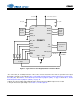
CS8421CS8421
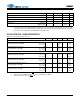
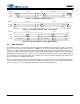
DIGITAL FILTER CHARACTERISTICS
3. The equation for the group delay through the sample-rate converter is (56.581 / Fsi) + (55.658 / Fso). For example,
if the input sample rate is 192 kHz and the output sample rate is 96 kHz, the group delay through the sample-rate
converter is (56.581/192,000) + (55.658/96,000) =.875 milliseconds.
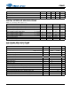
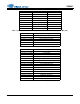
DC ELECTRICAL CHARACTERISTICS
(GND = 0 V; all voltages with respect to 0 V.)
4. Power Down Mode is defined as RST
= LOW with all clocks and data lines held static, except when a crystal is
attached across XTI-XTO, in which case the crystal will begin oscillating.
5. Normal operation is defined as RST
= HI.
Parameter Min Typ Max Units
Passband (Upsampling or Downsampling) - - 0.4535*Fso Hz
Passband Ripple - - ±0.007 dB
Stopband 0.5465*Fso - - Hz
Stopband Attenuation 125 - - dB
Group Delay SRC Mode
Bypass Mode
-
-
(Note 3)
-
-
3/Fsi
s
s
Parameter Symbol Min Typ Max Units
Power-Down Mode (Note 4)
Supply Current in power-down VD
(Oscillator attached to XTI-XTO) VL = 3.3 V
VL = 5.0 V
50
100
200
A
A
A
Supply Current in power-down VD
(Crystal attached to XTI-XTO) VL = 3.3 V
VL = 5.0 V
100
1.5
4
A
mA
mA
Normal Operation (Note 5)
Supply Current at 48 kHz Fsi and Fso VD
(Oscillator attached to XTI-XTO) VL = 3.3 V
VL = 5.0 V
24
2.5
4
mA
mA
mA
Supply Current at 192 kHz Fsi and Fso VD
(Oscillator attached to XTI-XTO) VL = 3.3 V
VL = 5.0 V
80
8
13
mA
mA
mA
Supply Current at 48 kHz Fsi and Fso VD
(Crystal attached to XTI-XTO) VL = 3.3 V
VL = 5.0 V
24
3
7
mA
mA
mA
Supply Current at 192 kHz Fsi and Fso VD
(Crystal attached to XTI-XTO) VL = 3.3 V
VL = 5.0 V
80
4
6.5
mA
mA
mA