CS8421 32-bit, 192-kHz Asynchronous Sample Rate Converter Features 175 dB Dynamic Range Bypass Mode –140 dB THD+N Time Division Multiplexing (TDM) Mode No Programming Required Attenuates Clock Jitter Multiple Device Outputs are Phase Matched No External Master Clock Required Linear Phase FIR Filter Supports Sample Rates up to 211 kHz Automatic Soft Mute/Unmute Input/Output Sample Rate Ratios of 7.5:1 to 1:8 +2.
CS8421 General Description The CS8421 is a 32-bit, high-performance, monolithic CMOS stereo asynchronous sample-rate converter. Digital audio inputs and outputs can be 32, 24, 20, or 16 bits. Input and output data can be completely asynchronous, synchronous to an external data clock, or the part can operate without any external clock by using an integrated oscillator. Audio data is input and output through configurable 3-wire input/output ports.
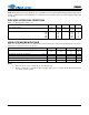
CS8421 TABLE OF CONTENTS 1. PIN DESCRIPTIONS ............................................................................................................................ 5 1.1 TSSOP Pin Descriptions ................................................................................................................ 5 1.2 QFN Pin Descriptions ..................................................................................................................... 7 2. CHARACTERISTICS AND SPECIFICATIONS ...............
CS8421 Figure 18. Wideband FFT Plot (16k Points) 0 dBFS 1 kHz Tone, 48 kHz:44.1 kHz .................................. 24 Figure 19. Wideband FFT Plot (16k Points) 0 dBFS 1 kHz Tone, 48 kHz:96 kHz ..................................... 24 Figure 20. Wideband FFT Plot (16k Points) 0 dBFS 1 kHz Tone, 96 kHz:48 kHz ..................................... 24 Figure 21. Wideband FFT Plot (16k Points) 0 dBFS 1 kHz Tone, 192 kHz:48 kHz ................................... 25 Figure 22.
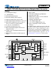
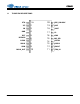
CS8421 1. PIN DESCRIPTIONS 1.
CS8421 6 Pin Name # XTO 1 Crystal Out (Output) - Crystal output for Master clock. See “Master Clock” on page 20. Pin Description XTI 2 Crystal/Oscillator In (Input) - Crystal or digital clock input for Master clock. See “Master Clock” on page 20. VD 3 Digital Power (Input) - Digital core power supply. Typically +2.5 V. GND 4 Ground (Input) - Ground for I/O and core logic. RST 5 Reset (Input) - When RST is low, the CS8421 enters a low-power mode and all internal states are reset.
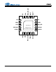
CS8421 DS641F6 XTI XTO SRC_UNLOC SAIF SAOF QFN PIN DESCRIPTIONS 20 19 18 17 16 GND 2 14 GND RST 3 Thermal Pad 13 MS_SEL BYPASS 4 Top-Down View 20-pin QFN Package 12 OLRCK ILRCK 5 11 OSCLK 6 7 8 9 10 SDOUT VL TDM_IN 15 MCLK_OUT 1 SDIN VD ISCLK 1.
CS8421 8 Pin Name # VD 1 Digital Power (Input) - Digital core power supply. Typically +2.5 V. Pin Description GND 2 Ground (Input) - Ground for I/O and core logic. RST 3 Reset (Input) - When RST is low, the CS8421 enters a low-power mode and all internal states are reset. On initial power-up, RST must be held low until the power supply is stable and all input clocks are stable in frequency and phase.
CS8421 2. CHARACTERISTICS AND SPECIFICATIONS (All Min/Max characteristics and specifications are guaranteed over the Specified Operating Conditions. Typical performance characteristics and specifications are derived from measurements taken at nominal supply voltages and TA = 25°C.) SPECIFIED OPERATING CONDITIONS (GND = 0 V, all voltages with respect to 0 V) Parameter Power Supply Voltage Ambient Operating Temperature: ‘-CZ’ ‘-CNZ’ ‘-DZ’ ‘-EZ’ ‘-ENZ’ Symbol Min Nominal Max Units VD VL 2.38 3.14 2.
CS8421 PERFORMANCE SPECIFICATIONS (XTI/XTO = 27 MHz; Input signal = 1.000 kHz, 0 dBFS, Measurement Bandwidth = 20 to Fso/2 Hz, and Word Width = 32-Bits, unless otherwise stated.) Parameter Resolution Min Typ 16 - 32 bits 7.2 53 - 207 211 kHz kHz - XTI/130 XTI/128 kHz kHz kHz Sample Rate with XTI = 27.
CS8421 DIGITAL FILTER CHARACTERISTICS Parameter Passband (Upsampling or Downsampling) Passband Ripple Stopband Stopband Attenuation Group Delay 3. SRC Mode Bypass Mode Min Typ Max Units - - 0.4535*Fso Hz - - ±0.007 dB 0.5465*Fso - - Hz 125 - - dB - (Note 3) - 3/Fsi s s The equation for the group delay through the sample-rate converter is (56.581 / Fsi) + (55.658 / Fso).
CS8421 DIGITAL INPUT CHARACTERISTICS Symbol Min Typ Max Units Input Leakage Current Parameters Iin - - ±10 A Input Capacitance Iin - 8 - pF - 250 - mV Input Hysteresis DIGITAL INTERFACE SPECIFICATIONS (GND = 0 V; all voltages with respect to 0 V.) Parameters Symbol Min Max Units High-Level Output Voltage, except MCLK_OUT and SDOUT (IOH=-4 mA) VOH 0.77xVL - V Low-Level Output Voltage, except MCLK_OUT and SDOUT (IOL=4 mA) VOL - .
CS8421 Parameters Symbol Min Max Units Master Mode (Note 9) I/OSCLK Frequency (non-TDM) 64*Fsi/o OSCLK Frequency (TDM) MHz 256*Fso I/OLRCK Duty Cycle I/OSCLK Duty Cycle MHz 45 55 % 45 55 % I/OSCLK Falling Edge to I/OLRCK Edge tlcks - 5 ns OSCLK Falling Edge to OLRCK Edge (TDM) tfss - 5 ns OSCLK Falling Edge to SDOUT Output Valid tdpd - 7 ns SDIN/TDM_IN Setup Time Before I/OSCLK Rising Edge tds 3 - ns SDIN/TDM_IN Hold Time After I/OSCLK Rising Edge tdh 5 - ns tlrckh
CS8421 3. TYPICAL CONNECTION DIAGRAMS +2.5 V +3.3 V or +5.0 V 0.1 F 0.1 F VD Serial Audio Source VL ILRCK OLRCK ISCLK OSCLK SDIN SDOUT Serial Audio Input Device *** TDM_IN MS_SEL CS8421 SAIF XTI 1 k * SAOF SRC_UNLOCK BYPASS ** RST GND GND Hardware Control Settings Figure 5. Typical Connection Diagram, No External Master Clock * When no external master clock is supplied to the part, both input and output must be set to Slave Mode for the part to operate properly.
CS8421 +2.5 V +3.3 V or +5.0 V 0.1 F 0.1 F VD Serial Audio Source VL ILRCK OLRCK ISCLK OSCLK SDIN SDOUT Serial Audio Input Device *** TDM_IN MS_SEL CS8421 SAIF XTI Crystal /Clock Source SAOF XTO SRC_UNLOCK BYPASS MCLK_OUT * RST 47 k GND ** GND To external hardware Hardware Control Settings Figure 6.
CS8421 4. APPLICATIONS The CS8421 is a 32-bit, high-performance, monolithic CMOS stereo asynchronous sample-rate converter. The digital audio data is input and output through configurable 3-wire serial ports. The digital audio input/output ports offer Left-Justified, Right-Justified, and I²S serial audio formats. The CS8421 also supports a TDM Mode which allows multiple channels of digital audio data on one serial line.
CS8421 I/OLRCK Channel A Channel B I/OSCLK SDIN SDOUT M SB MSB LSB MSB LSB Figure 7. Serial Audio Interface Format - I²S I/OLRCK Channel A Channel B I/OSCLK SDIN SDOUT M SB MSB LSB MSB LSB Figure 8. Serial Audio Interface Format - Left-Justified I/OLRCK Channel A Channel B I/OSCLK SDIN SDOUT MSB Extended MSB LSB MSB LSB MSB Extended MSB LSB MSB LSB Figure 9. Serial Audio Interface Format - Right-Justified 4.
CS8421 MS_SEL pin 1.0 k ± 1% to GND Input M/S Slave Output M/S Slave 1.96 k ± 1% to GND Slave Master (128 x Fso) 4.02 k ± 1% to GND Slave Master (256 x Fso) 8.06 k ± 1% to GND Slave Master (384 x Fso) 16.2 k ± 1% to GND Slave Master (512 x Fso) 1.0 k ± 1% to VL Master (128 x Fsi) Slave 1.96 k ± 1% to VL Master (256 x Fsi) Slave 4.02 k ± 1% to VL Master (384 x Fsi) Slave Slave 8.06 k ± 1% to VL Master (512 x Fsi) Table 1.
CS8421 4.3 Sample Rate Converter (SRC) Multirate digital signal processing techniques are used to conceptually upsample the incoming data to a very high rate and then downsample to the outgoing rate. The internal data path is 32-bits wide even if a lower bit depth is selected at the output. The filtering is designed so that a full input audio bandwidth of 20 kHz is preserved if the input sample and output sample rates are greater than or equal to 44.1 kHz.
CS8421 4.3.4 Muting The SDOUT pin is set to all zero output (full mute) immediately after the RST pin is set high. When the output from the SRC becomes valid, though the SRC may not have reached full performance, SDOUT is unmuted over a period of approximately 4096 OLRCK cycles (soft unmuted).
CS8421 4.3.7 Clocking In order to ensure proper operation of the CS8421, the clock or crystal attached to XTI must simultaneously satisfy the requirements of LRCK for both the input and output as follows: • If the input is set to master, Fsi XTI/128 and Fso XTI/130. • If the output is set to master, Fso XTI/128 and Fsi XTI/130. • If both input and output are set to slave, XTI 130*[maximum(Fsi,Fso)], XTI/Fsi < 3750, and XTI/Fso < 3750. XTI XTO R C C Figure 10.
CS8421 256 OSCLKs OLRCK OSCLK SDOUT/ TDM_IN MSB LSB MSB LSB MSB LSB MSB LSB MSB LSB MSB LSB MSB LSB MSB LSB SDOUT 4, ch A SDOUT 4, ch B SDOUT 3, ch A SDOUT 3, ch B SDOUT 2, ch A SDOUT 2, ch B SDOUT 1, ch A SDOUT 1, ch B 32 clks 32 clks 32 clks 32 clks 32 clks 32 clks 32 clks 32 clks Figure 12.
CS8421 4.6 Power Supply, Grounding, and PCB Layout The CS8421 operates from a VD = +2.5 V and VL = +3.3 V or +5.0 V supply. These supplies may be set independently. Follow normal supply decoupling practices; see Figure 6. Extensive use of power and ground planes, ground-plane fill in unused areas, and surface-mount decoupling capacitors are recommended.
CS8421 5. PERFORMANCE PLOTS d B F S +0 +0 -20 -20 -40 -40 -60 -60 -80 d B F S -100 -120 -80 -100 -120 -140 -140 -160 -160 -180 -180 -200 5k 10k 15k -200 20k 20k 40k Figure 15. Wideband FFT Plot (16k Points) 0 dBFS d B F S +0 +0 -20 -40 -40 -60 -60 -80 d B F S -100 -120 -80 -100 -120 -140 -140 -160 -160 -180 -180 5k 10k 15k -200 20k 2.5k 5k 7.
CS8421 +0 -60 -20 -40 -80 -60 -100 -80 d B F S d B F S -100 -120 -140 -120 -140 -160 -160 -180 -180 -200 5k 10k 15k -200 20k 10k 20k Figure 21. Wideband FFT Plot (16k Points) 0 dBFS d B F S -60 -80 -80 -100 -100 d B F S -120 -140 -120 -140 -160 -160 -180 -180 5k 10k 15k -200 20k 20k 40k Hz -60 -80 -80 -100 -100 d B F S -120 -140 -120 -140 -160 -160 -180 -180 5k 10k 15k 20k Hz Figure 25.
CS8421 +0 -60 -20 -80 -40 -60 -100 d B F S d B F S -120 -140 -80 -100 -120 -140 -160 -160 -180 -200 -180 5k 10k 15k -200 20k 5k 10k Hz 15k 20k Hz Figure 27. Wideband FFT Plot (16k Points) - 60 dBFS 1 kHz Tone, 96 kHz:48 kHz +0 -60 -20 -40 -80 -60 -100 d B F S d B F S -120 -140 -80 -100 -120 -140 -160 -160 -180 -200 -180 5k 10k 15k -200 20k 2.5k 5k 7.5k 10k Figure 29.
CS8421 d B F S +0 +0 -20 -20 -40 -40 -60 -60 -80 d B F S -100 -120 -80 -100 -120 -140 -140 -160 -160 -180 -180 -200 20k 40k 60k -200 80k 10k 20k Figure 33. Wideband FFT Plot (16k Points) 0 dBFS d B F S +0 +0 -20 -40 -40 -60 -60 -80 d B F S -100 -120 -80 -100 -120 -140 -140 -160 -160 -180 -180 5k 10k 40k 80 kHz Tone, 192 kHz:192 kHz -20 -200 30k Hz Hz 15k -200 20k 5k 10k Hz 15k 20k Hz Figure 35.
CS8421 d B F S -120 -120 -122.5 -122.5 -125 -125 -127.5 -127.5 -130 -130 -132.5 -132.5 d B F S -135 -137.5 -135 -137.5 -140 -140 -142.5 -142.5 -145 -145 -147.5 -147.5 -150 50k 75k 100k 125k 150k -150 175k 50k 75k 100k 125k 150k 175k Hz Hz Figure 39. THD+N vs. Output Sample Rate, 0 dBFS 1 kHz Tone, Fsi = 48 kHz -120 -135 -122.5 -136 -125 -137 -127.5 -138 -130 d B F S -132.5 d B F S -135 -137.5 -140 -139 -140 -141 -142 -142.5 -143 -145 -144 -147.
CS8421 -120 -120 -122.5 -122.5 -125 -125 -127.5 -127.5 -130 d B F S -130 -132.5 d B F S -135 -137.5 -132.5 -135 -137.5 -140 -140 -142.5 -142.5 -145 -145 -147.5 -147.5 -150 50k 75k 100k 125k 150k -150 175k 50k 75k 100k Hz 125k 150k 175k Hz Figure 45. Dynamic Range vs. Output Sample Rate, -60 dBFS 1 kHz Tone, Fsi = 96 kHz +0 +0 -0.02 -20 -0.04 -40 d B F S -0.06 192 kHz:48 kHz -60 d B F S 192 kHz:96 kHz -80 -100 -0.08 -0.1 -0.12 -0.14 192 kHz:32 kHz -0.
CS8421 +0 +0 -10 -10 -20 -20 -30 -30 -40 -40 -50 -50 d B F S d B F S -60 -70 -80 -60 -70 -80 -90 -90 -100 -100 -110 -110 -120 -120 -130 -130 -140 -140 -120 -100 -80 -60 -40 -20 -140 -140 +0 -120 -100 -80 Figure 51.
CS8421 -110 -110 -115 -115 -120 -120 -125 -125 -130 -130 -135 -135 d B F S -140 d B F S -145 -150 -140 -145 -150 -155 -155 -160 -160 -165 -165 -170 -170 -175 -175 -180 -140 -120 -100 -80 -60 -40 -20 -180 -140 +0 -120 -100 -80 dBFS Figure 57. THD+N vs.
CS8421 -110 -110 -115 -115 -120 -120 -125 -125 -130 -130 -135 -135 d B F S -140 d B F S -145 -150 -140 -145 -150 -155 -155 -160 -160 -165 -165 -170 -170 -175 -175 -180 0 -180 2.5k 5k 7.5k 10k 12.5k 15k 17.5k 20k -140 -120 -100 Figure 63. THD+N vs.
CS8421 6. PACKAGE DIMENSIONS 20L TSSOP (4.4 MM BODY) PACKAGE DRAWING N D E11 A2 E A e A1 2 b END VIEW L SIDE VIEW SEATING PLANE 1 2 3 TOP VIEW INCHES DIM A A1 A2 b D E E1 e L µ MIN -0.002 0.03346 0.00748 0.252 0.248 0.169 -0.020 0° NOM -0.004 0.0354 0.0096 0.256 0.2519 0.1732 -0.024 4° NOTE MILLIMETERS MAX 0.043 0.006 0.037 0.012 0.259 0.256 0.177 0.026 0.028 8° MIN -0.05 0.85 0.19 6.40 6.30 4.30 -0.50 0° NOM --0.90 0.245 6.50 6.40 4.40 -0.60 4° MAX 1.10 0.15 0.95 0.30 6.60 6.50 4.
CS8421 20-PIN QFN (5 5 MM BODY) PACKAGE DRAWING b D Pin #1 Corner e Pin #1 Corner E2 E A1 D2 L A Top View DIM A A1 b D D2 E E2 e L Side View MIN -0.0000 0.0091 0.1201 0.1202 0.0197 INCHES NOM --0.0110 0.1969 BSC 0.1220 0.1969 BSC 0.1221 0.0256 BSC 0.0236 Bottom View MAX 0.0394 0.0020 0.0130 MIN -0.00 0.23 0.1240 3.05 0.1241 3.05 0.0276 0.50 MILLIMETERS NOM --0.28 5.00 BSC 3.10 5.00 BSC 3.10 0.65 BSC 0.60 NOTE MAX 1.00 0.05 0.33 3.15 3.15 0.
CS8421 7. ORDERING INFORMATION Product Description CS8421 Package Pb-Free Temp Range 20-TSSOP -10° to +70°C 20-QFN 32-bit Asynchronous Sample Rate Converter 20-TSSOP YES -40° to +85°C 20-TSSOP -40° to +105°C 20-QFN CDB8421 Evaluation Board for CS8421 - - Container Order# Rail Tape and Reel Rail Tape and Reel Rail Tape and Reel Rail Tape and Reel Rail Tape and Reel - CS8421-CZZ CS8421-CZZR CS8421-CNZ CS8421-CNZR CS8421-DZZ CS8421-DZZR CS8421-EZZ CS8421-EZZR CS8421-ENZ CS8421-ENZR CDB8421 8.