
User guide

36 DS578F3
CS8416
14. CONTROL PORT REGISTER DESCRIPTIONS
14.1 Memory Address Pointer (MAP)
Not a register
MAP[6:0] - Memory Address Pointer. Will automatically increment after each read or write.
Default = ‘0000000’
14.2 Control0 (00h)
FSWCLK – Forces the clock signal on OMCK to be output on RMCK regardless of the SWCLK (Control1
register bit 6) bit functionality or PLL lock.
Default = ‘0’
0 – Clock signal on OMCK is output on RMCK according to the SWCLK bit functionality.
1 – Forces the clock signal on OMCK to be output on RMCK regardless of the SWCLK bit functionality.
PDUR – Changes the type of phase detector used to lock to the active RXP[7:0] input. This bit should only
be set if the sample rate range is between 32 kHz and 108 kHz. If the sample rate is outside of this range
and the PDUR bit is set, loss of lock may occur.
Default = ‘0’
0 – Normal Update Rate Phase Detector - Recovered master clock (RMCK) will have low wide-band jitter,
but increased in-band jitter.
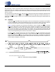
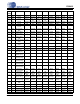
1E R Channel B Status BC0[7] BC0[6] BC0[5] BC0[4] BC0[3] BC0[2] BC0[1] BC0[0]
1F R Channel B Status BC1[7] BC1[6] BC1[5] BC1[4] BC1[3] BC1[2] BC1[1] BC1[0]
20 R Channel B Status BC2[7] BC2[6] BC2[5] BC2[4] BC2[3] BC2[2] BC2[1] BC2[0]
21 R Channel B Status BC3[7] BC3[6] BC3[5] BC3[4] BC3[3] BC3[2] BC3[1] BC3[0]
22 R Channel B Status BC4[7] BC4[6] BC4[5] BC4[4] BC4[3] BC4[2] BC4[1] BC4[0]
23 R Burst Preamble PC
Byte 0
PC0[7] PC0[6] PC0[5] PC0[4] PC0[3] PC0[2] PC0[1] PC0[0]
24 R Burst Preamble PC
Byte 1
PC1[7] PC1[6] PC1[5] PC1[4] PC1[3] PC1[2] PC1[1] PC1[0]
25 R Burst Preamble PD
Byte 0
PD0[7] PD0[6] PD0[5] PD0[4] PD0[3] PD0[2] PD0[1] PD0[0]
26 R Burst Preamble PD
Byte 1
PD1[7] PD1[6] PD1[5] PD1[4] PD1[3] PD1[2] PD1[1] PD1[0]
7F R ID & Version ID3 ID2 ID1 ID0 VER3 VER2 VER1 VER0
76543210
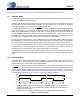
0 MAP6MAP5MAP4MAP3MAP2MAP1MAP0
76543210
0 FSWCLK 0 0 PDUR TRUNC Reserved Reserved
Addr
(HEX)
R/WFunction76543210