
User guide

DS578F3 21
CS8416
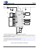
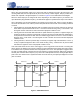
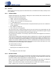
Figure 6. Typical Connection Diagram - Hardware Mode
* These pins must be pulled high to VL or low to DGND through a 47 kΩ resistor.
** A separate analog supply is only necessary in applications where RMCK is used for a jitter sensitive task. For
applications where RMCK is not used for a jitter sensitive task, connect VA to VD via a ferrite bead. Keep decou-
pling capacitors between VA and AGND.
*** See “S/PDIF Receiver” on page 27 and “External AES3/SPDIF/IEC60958 Receiver Components” on page 49
for typical input configurations and recommended input circuits.
**** For best jitter performance connect the filter ground directly to the AGND pin. See Table 6 on page 54 for PLL
filter values.
10 Fμ
CS8416
0.1 Fμ
+3.3 V
FILT DGNDAGND
R
FLT
C
FLT
C
RIP
***
****
RXN
RXP0
RXP1
RXP2
RXP3
AES3 /
S/PDIF
Sources
Hardware
Control
RXSEL1
TXSEL0
TXSEL1
NV/RERR
96KHZ
RCBL
U
C
Ferrite
Bead
+3.3 V
Analog
Supply
**
OMCK Clock Source
RXSEL0
RST
AUDIO
VA
VD
VL
TX
RMCK
Clock Control
Serial Audio
Input Device
OLRCK
OSCLK
SDOUT
External
Interface
47k Ω
**
*
*
*
*
*
*
0.1 Fμ
0.1 Fμ
+3.3 V or +5 V
VL
VL
*