
User guide

18 DS578F3
CS8416
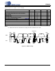
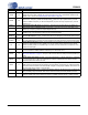
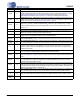
3.2 QFN Pin Description
Pin Name Pin # Pin Description
VA 3
Analog Power (Input) - Analog power supply. Nominally +3.3 V. This supply should have as little
noise as possible since noise on this pin will directly affect the jitter performance of the recovered
clock
VD 20 Digital Power (Input) – Digital core power supply. Nominally +3.3 V
VL 18 Logic Power (Input) – Input/Output power supply. Nominally +3.3 V or +5.0 V
AGND 4
Analog Ground (Input) - Ground for the analog circuitry in the chip. AGND and DGND should be
connected to a common ground area under the chip.
DGND 19
Digital & I/O Ground (Input) - Ground for the I/O and core logic. AGND and DGND should be con-
nected to a common ground area under the chip.
RST
6
Reset (Input) - When RST
is low, the CS8416 enters a low power mode and all internal states are
reset. On initial power up, RST
must be held low until the power supply is stable, and all input clocks
are stable in frequency and phase.
FILT 5
PLL Loop Filter (Output) - An RC network should be connected between this pin and analog
ground.
For minimum PLL jitter, return the ground end of the filter network directly to AGND. See “PLL Filter”
on page 53 for more information on the PLL and the external components.
RXP0
RXP1
RXP2
RXP3
1
28
27
26
Positive AES3/SPDIF Input (Input) - Single-ended or differential receiver inputs carrying AES3 or
S/PDIF encoded digital data. The RXP[3:0] inputs comprise the 4:2 S/PDIF Input Multiplexer. The
select line control is accessed using the RXPSEL[1:0] pins. Unused multiplexer inputs should be left
floating or tied to AGND. See “External AES3/SPDIF/IEC60958 Receiver Components” on page 49
for recommended input circuits.
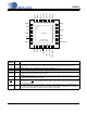
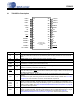
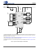
98
7
6
5
4
3
2
1
10
11
12 13 14
15
16
17
18
19
20
21
222324
25
262728
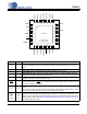
Top-Down View
28-pin QFN Package
Thermal Pad
RXP1
RXP2
RXP3
OLRCK
OSCLK
SDOUT
OMCK
RXSEL0
TXSEL1
TXSEL0
NV / RERR
AUDIO
96KHZ
RCBL
RXP0
RXN
VA
AGND
FILT
RST
RXSEL1
RMCK
VD
DGND
VL
TX
C
U