CS8416 192 kHz Digital Audio Interface Receiver Features 32 kHz to 192 kHz Sample Frequency Range Complete EIAJ CP1201, IEC-60958, AES3, Low-Jitter Clock Recovery S/PDIF-Compatible Receiver Pin and Microcontroller Read Access to +3.3 V Analog Supply (VA) Channel Status and User Data +3.3 V Digital Supply (VD) SPI™ or I²C® Control Port Software Mode and Stand-Alone Hardware Mode +3.3 V or +5.
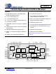
CS8416 General Description The CS8416 is a monolithic CMOS device that receives and decodes one of eight stereo pairs of digital audio data according to the IEC60958, S/PDIF, EIAJ CP1201, or AES3 interface standards. The CS8416 has a serial digital audio output port and comprehensive control ability through a selectable control port in Software Mode or through selectable pins in Hardware Mode. Channel status data are assembled in buffers, making read access easy.
CS8416 TABLE OF CONTENTS 1. CHARACTERISTICS AND SPECIFICATIONS ..................................................................................... 6 SPECIFIED OPERATING CONDITIONS ............................................................................................... 6 ABSOLUTE MAXIMUM RATINGS ......................................................................................................... 6 DC ELECTRICAL CHARACTERISTICS......................................................................
CS8416 14.4 Control2 (02h) ............................................................................................................................. 38 14.5 Control3 (03h) ............................................................................................................................. 39 14.6 Control4 (04h) ............................................................................................................................. 39 14.7 Serial Audio Data Format (05h) ......................
CS8416 LIST OF FIGURES Figure 1. Audio Port Master Mode Timing ................................................................................................... 9 Figure 2. Audio Port Slave Mode and Data Input Timing............................................................................. 9 Figure 3. SPI Mode Timing ........................................................................................................................ 10 Figure 4. I²C Mode Timing ......................................
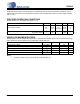
CS8416 1. CHARACTERISTICS AND SPECIFICATIONS All Min/Max characteristics and specifications are guaranteed over the Specified Operating Conditions. Typical performance characteristics and specifications are derived from measurements taken at nominal supply voltages and TA = 25°C. SPECIFIED OPERATING CONDITIONS (AGND, DGND = 0 V, all voltages with respect to 0 V) Parameter Power Supply Voltage Ambient Operating Temperature: Commercial Grade Automotive Grade Symbol Min Typ Max Units VA VD VL 3.13 3.
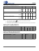
CS8416 DC ELECTRICAL CHARACTERISTICS (AGND = DGND = 0 V; all voltages with respect to 0 V.) Parameters Symbol Min Typ Max Units VA VD VL = 3.3 V VL = 5.0 V IA ID IL IL - 10 70 10 12 - μA μA μA μA VA VD VL = 3.3 V VL = 5.0 V VA VD VL = 3.3 V VL = 5.0 V IA ID IL IL IA ID IL IL - 5.7 5.9 2.8 4.2 9.4 23 7.8 11.
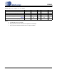
CS8416 SWITCHING CHARACTERISTICS (Inputs: Logic 0 = 0 V, Logic 1 = VL; CL = 20 pF) Parameter Symbol Min Typ Max Units RST Pin Low Pulse Width 200 - - μS PLL Clock Recovery Sample Rate Range 30 - 200 kHz RMCK Output Jitter (Note 5) - 200 - ps RMS RMCK Output Duty-Cycle (Note 6) (Note 7) 45 50 50 55 55 65 % % - - 50 MHz RMCK/OMCK Maximum Frequency Notes: 5. Typical RMS cycle-to-cycle jitter. 6. Duty cycle when clock is recovered from biphase encoded input. 7.
CS8416 SWITCHING CHARACTERISTICS - SERIAL AUDIO PORTS (Inputs: Logic 0 = 0 V, Logic 1 = VL; CL = 20 pF) Parameter Symbol Min Typ Max Units OSCLK/OLRCK Active Edge to SDOUT Output Valid (Note 8) Master Mode RMCK to OSCLK active edge delay (Note 8) RMCK to OLRCK delay (Note 9) OSCLK and OLRCK Duty Cycle Slave Mode OSCLK Period OSCLK Input Low Width OSCLK Input High Width OSCLK Active Edge to OLRCK Edge (Notes 8,9,10) OSCLK Edge Setup Before OSCLK Active-Edge (Notes 8,9,11) tdpd - - 23 ns tsmd tlmd
CS8416 SWITCHING CHARACTERISTICS - CONTROL PORT - SPI MODE (Inputs: Logic 0 = 0 V, Logic 1 = VL; CL = 20 pF) Parameter Symbol Min Max Unit fsck 0 6.0 MHz CS High Time Between Transmissions tcsh 1.
CS8416 SWITCHING CHARACTERISTICS - CONTROL PORT- I²C FORMAT (Inputs: Logic 0 = 0 V, Logic 1 = VL; CL = 20 pF) Parameter Symbol Min Max Unit SCL Clock Frequency Bus Free Time Between Transmissions Start Condition Hold Time (prior to first clock pulse) Clock Low time Clock High Time Setup Time for Repeated Start Condition SDA Hold Time from SCL Falling (Note 15) SDA Setup time to SCL Rising Rise Time of SCL and SDA Fall Time SCL and SDA Setup Time for Stop Condition fscl tbuf thdst tlow thigh tsust thdd
CS8416 2. PIN DESCRIPTION - SOFTWARE MODE 2.1 12 TSSOP Pin Description RXP3 1 28 OLRCK RXP2 2 27 OSCLK RXP1 3 26 SDOUT RXP0 4 25 OMCK RXN 5 24 RMCK VA 6 23 VD AGND 7 22 DGND FILT 8 21 VL RST 9 20 GPO0 RXP4 10 19 GPO1 RXP5 11 18 AD2 / GPO2 RXP6 12 17 SDA / CDOUT RXP7 13 16 SCL / CCLK AD0 / CS 14 15 AD1 / CDIN Top-Down View 28-pin SOIC/TSSOP Package Pin Name Pin # Pin Description VA 6 Analog Power (Input) - Analog power supply. Nominally +3.3 V.
CS8416 Pin Name Pin # Pin Description 5 Negative AES3/SPDIF Input (Input) - Single-ended or differential receiver input carrying AES3 or S/PDIF encoded digital data. Used along with RXP[7:0] to form an AES3 differential input. In singleended operation this should be AC coupled to ground through a capacitor. See “External AES3/SPDIF/IEC60958 Receiver Components” on page 49 for recommended input circuits.
CS8416 14 RXP1 RXP2 RXP3 OLRCK OSCLK SDOUT OMCK QFN Pin Description 28 27 26 25 24 23 22 RXP0 1 21 RMCK RXN 2 20 VD VA 3 19 DGND AGND 4 18 VL FILT 5 17 GPO0 RST 6 16 GPO1 RXP4 7 15 AD2 / GPO2 Thermal Pad 11 RXP7 AD0 / CS 12 13 14 SDA / CDOUT 10 SCL / CCLK 9 AD1 / CDIN 8 RXP6 Top-Down View 28-pin QFN Package RXP5 2.2 Pin Name Pin # Pin Description VA 3 Analog Power (Input) - Analog power supply. Nominally +3.3 V.
CS8416 Pin Name Pin # Pin Description RXP0 RXP1 RXP2 RXP3 RXP4 RXP5 RXP6 RXP7 1 28 27 26 7 8 9 10 Positive AES3/SPDIF Input (Input) - Single-ended or differential receiver inputs carrying AES3 or S/PDIF encoded digital data. The RXP[7:0] inputs comprise the 8:2 S/PDIF Input Multiplexer. The select line control is accessed using the Control 4 register (04h). Unused multiplexer inputs should be left floating or tied to AGND.
CS8416 3. PIN DESCRIPTION - HARDWARE MODE 3.1 TSSOP Pin Description Pin Name Pin # VA 6 1 28 OLRCK RXP2 2 27 OSCLK RXP1 3 26 SDOUT RXP0 4 25 OMCK RXN 5 24 RMCK VA 6 23 VD AGND 7 22 DGND FILT 8 21 VL RST 9 20 TX RXSEL1 10 19 C RXSEL0 11 18 U TXSEL1 12 17 RCBL TXSEL0 13 16 96KHZ NV / RERR 14 15 AUDIO Top-Down View 28-pin SOIC/TSSOP Package Pin Description Analog Power (Input) - Analog power supply. Nominally +3.3 V.
CS8416 Pin Name Pin # Pin Description OMCK 25 System Clock (Input) - OMCK System Clock Mode is enabled by a transition (rising edge active) on OMCK after reset. When enabled, the clock signal input on this pin is automatically output through RMCK on PLL unlock. See “OMCK System Clock Mode” on page 28. RMCK 24 Input Section Recovered Master Clock (Output) - Input section recovered master clock output from the PLL.
CS8416 RXP1 RXP2 RXP3 OLRCK OSCLK SDOUT OMCK QFN Pin Description 28 27 26 25 24 23 22 RXP0 1 21 RMCK RXN 2 20 VD VA 3 19 DGND AGND 4 18 VL FILT 5 17 TX RST 6 16 C RXSEL1 7 15 U Thermal Pad 11 TXSEL0 NV / RERR 12 13 14 RCBL 10 96KHZ 9 AUDIO 8 TXSEL1 Top-Down View 28-pin QFN Package RXSEL0 3.2 Pin Name Pin # VA 3 Analog Power (Input) - Analog power supply. Nominally +3.3 V.
CS8416 Pin Name Pin # Pin Description RXN 2 Negative AES3/SPDIF Input (Input) - Single-ended or differential receiver input carrying AES3 or S/PDIF encoded digital data. Used along with RXP[3:0] to form an AES3 differential input. In singleended operation this should be AC coupled to ground through a capacitor. See “External AES3/SPDIF/IEC60958 Receiver Components” on page 49 for recommended input circuits.
CS8416 4. TYPICAL CONNECTION DIAGRAMS +3.3 V Analog Supply Ferrite Bead * +3.3 V +3.3 V or +5 V * 10 μ F 0.1μ F 0.1μ F VA 0.
CS8416 +3.3 V Analog Supply Ferrite ** Bead +3.3 V +3.3 V or +5 V ** 10 μ F 0.1μ F VD VA VL VL OLRCK RXN *** AES3 / S/PDIF Sources 0.1μ F 0.
CS8416 5. APPLICATIONS 5.1 Reset, Power-Down and Start-Up When RST is low, the CS8416 enters a low power mode and all internal states are reset, including the control port and registers, and the outputs are muted. In Software Mode, when RST is high, the control port becomes operational, and the desired settings should be loaded into the control registers. Writing a 1 to the RUN bit will then cause the part to leave the low power state and begin operation.
CS8416 6. GENERAL DESCRIPTION The CS8416 is a monolithic CMOS device that receives and decodes audio data according to the AES3, IEC60958, S/PDIF, and EIAJ CP1201 interface standards. The CS8416 provides an 8:2 multiplexer to select between eight inputs for decoding and to allow an input signal to be routed to an output of the CS8416. Input data can be either differential or single-ended. A low jitter clock is recovered from the incoming data using a PLL.
CS8416 clock all the data bits. When in slave mode, the serial audio output port cannot be set for right-justified data. The CS8416 allows immediate mute of the serial audio output port audio data by the MUTESAO bit of Control Register 1. For more information about serial audio formats, refer to the Cirrus Logic applications note AN282, “The 2-Channel Serial Audio Interface: A Tutorial”, available at www.cirrus.com.
CS8416 7.1 Slip/Repeat Behavior When using the serial audio output port in slave mode with an OLRCK input that is asynchronous to the incoming AES3 data, the interrupt bit OSLIP (bit 5 in the Interrupt 1 Status register, 0Dh) is provided to indicate when repeated or dropped samples occur. Refer to Figure 8 for the AES3 data format diagram.
CS8416 7.2 AES11 Behavior When OLRCK is configured as a master, the positive or negative edge of OLRCK (depending on the setting of SOLRPOL in register 05h) will be within -1.0%(1/Fs) to 1.1%(1/Fs) from the start of the preamble X/Z. In master mode, the latency through the part is dependent on the input sample frequency. The typical delay through the part from the beginning of the preamble to the active edge of OLRCK for the various sample frequencies is given in Table 1.
CS8416 8. S/PDIF RECEIVER The CS8416 includes an AES3/SPDIF digital audio receiver. The receiver accepts and decodes bi-phase encoded audio and digital data according to the AES3, IEC60958 (S/PDIF), and EIAJ CP-1201 interface standards. The receiver consists of an analog differential input stage, driven through analog input pins RXP0 to RXP7 and a common RXN, a PLL based clock recovery circuit, and a decoder which separates the audio data from the channel status and user data.
CS8416 The second output of the input multiplexer is used to provide the selected input as a source to be output on a GPO pin. This pass through signal is selected by TXSEL[2:0] in control port register 04h. This singleended signal is resolved to full-rail, but is not de-jittered before it is output. 8.1.3 Hardware Mode In Hardware Mode the input to the decoder is selected by dedicated pins, RXSEL[1:0]. The pass through signal is selected by dedicated pins, TXSEL[1:0] for output on the dedicated TX pin.
CS8416 9. GENERAL PURPOSE OUTPUTS Three General Purpose Outputs (GPO) are provided to allow the equipment designer flexibility in configuring the CS8416. Fourteen signals are available to be routed to any of the GPO pins. The outputs of the GPO pins are set through the GPOxSEL[3:0] bits in the Control2 (02h) and Control3 (03h) registers. All GPO pins default to GND after reset.
CS8416 10.ERROR AND STATUS REPORTING 10.1 General While decoding the incoming bi-phase encoded data stream, the CS8416 has the ability to identify various error conditions. 10.1.1 Software Mode Software Mode allows the most flexibility in reading errors. When unmasked, bits in the Receiver Error register (0Ch) indicate the following errors: 1. QCRC – CRC error in Q subcode data. 2. CCRC – CRC error in channel status data. 3. UNLOCK – PLL is not locked to incoming data stream. 4.
CS8416 10.2 Non-Audio Detection An AES3 data stream may be used to convey non-audio data, thus it is important to know whether the incoming AES3 data stream is digital audio or not. This information is typically conveyed in channel status bit 1, which is extracted automatically by the CS8416. However, certain non-audio sources, such as AC-3™ or MPEG encoders, may not adhere to this convention, and the bit may not be properly set.
CS8416 11.CHANNEL STATUS AND USER-DATA HANDLING “Channel Status Buffer Management” on page 51 describes Channel Status and User data control. 11.1 Software Mode In Software Mode, several options are available for accessing the Channel Status and User data that is encoded in the received AES3/SPDIF stream. The first option allows access directly through registers. The first 5 bytes of the Channel Status block are decoded into the Receiver Channel Status Registers 19h - 22h.
CS8416 12.CONTROL PORT DESCRIPTION The control port is used to access the registers, allowing the CS8416 to be configured for the desired operational modes and formats. The operation of the control port may be completely asynchronous with respect to the audio sample rates. However, to avoid potential interference problems, the control port pins should remain static if no operation is required. The control port has 2 modes: SPI and I²C, with the CS8416 acting as a slave device.
CS8416 12.2 I²C Mode In I²C Mode, SDA is a bidirectional data line. Data is clocked into and out of the part by the clock, SCL. There is no CS pin. Pins AD0 and AD1 form the two least significant bits of the chip address and should be connected through a resistor to VL or DGND as desired. The GPO2 pin is used to set the AD2 bit by connecting a 47 kΩ resistor from the GPO2 pin to VL or to DGND. The states of the pins are sensed while the CS8416 is being reset.
CS8416 13.
CS8416 Addr R/W (HEX) Function 7 6 5 4 3 2 1 0 1E R Channel B Status BC0[7] BC0[6] BC0[5] BC0[4] BC0[3] BC0[2] BC0[1] BC0[0] 1F R Channel B Status BC1[7] BC1[6] BC1[5] BC1[4] BC1[3] BC1[2] BC1[1] BC1[0] 20 R Channel B Status BC2[7] BC2[6] BC2[5] BC2[4] BC2[3] BC2[2] BC2[1] BC2[0] 21 R Channel B Status BC3[7] BC3[6] BC3[5] BC3[4] BC3[3] BC3[2] BC3[1] BC3[0] 22 R Channel B Status BC4[7] BC4[6] BC4[5] BC4[4] BC4[3] BC4[2] BC4[1] BC4[0] 23 R Bur
CS8416 1 – Higher Update Rate Phase Detector - Recovered master clock (RMCK) will have low in-band jitter, but increased wide-band jitter. Use this setting for the best performance when the output is connected to a deltasigma digital-to-analog converter (DAC). TRUNC – Determines if the audio word length is set according to the incoming channel status data as decoded by the AUX[3:0] bits. The resulting word length in bits is 24 minus AUX[3:0]. Default = ‘0’ 0 – Incoming data is not truncated.
CS8416 RMCKF – Recovered Master Clock Frequency Default = ‘0’ 0 – RMCK output frequency is 256*FS. 1 – RMCK output frequency is 128*FS. CHS – Sets which channel's C data is decoded in the Receiver Channel Status register (0Ah). Default = ‘0’ 0 – A channel. 1 – B channel. If CHS = 0 and TRUNC = 1, both channels' audio data will be truncated by the AUX[3:0] bits indicated in the channel A Channel Status data.
CS8416 Gain, dB T1 = 50us 0 T2 =15us -10 F1 3.183 Frequency, KHz F2 10.61 Figure 14. De-Emphasis Filter Response 14.5 Control3 (03h) 7 GPO1SEL3 6 GPO1SEL2 5 GPO1SEL1 4 GPO1SEL0 3 GPO2SEL3 2 GPO2SEL2 1 GPO2SEL1 0 GPO2SEL0 GPO1SEL[3:0] – GPO1 Source select. See “General Purpose Outputs” on page 29. Default = ‘0000’ GPO2SEL[3:0] – GPO2 Source select. See “General Purpose Outputs” on page 29. Default = ‘0000’ 14.
CS8416 TX_SEL[2:0] – Selects RXP0 to RXP7 as the input for GPO TX source Default =’001’ 000 – RXP0 001 – RXP1, etc 14.7 Serial Audio Data Format (05h) 7 SOMS 6 SOSF 5 SORES1 4 SORES0 3 SOJUST 2 SODEL 1 SOSPOL 0 SOLRPOL SOMS - Master/Slave Mode Selector Default = ‘0’ 0 - Serial audio output port is in slave mode. OSCLK and OLRCK are inputs. 1 - Serial audio output port is in master mode. OSCLK and OLRCK are outputs.
CS8416 SOLRPOL - OLRCK clock polarity Default = ‘0’ 0 - SDOUT data is valid for the left channel when OLRCK is high. 1 - SDOUT data is valid for the right channel when OLRCK is high. 14.8 Receiver Error Mask (06h) 7 0 6 QCRCM 5 CCRCM 4 UNLOCKM 3 VM 2 CONFM 1 BIPM 0 PARM The bits in this register serve as masks for the corresponding bits of the Receiver Error Register.
CS8416 14.11 Receiver Channel Status (0Ah) 7 AUX3 6 AUX2 5 AUX1 4 AUX0 3 PRO 2 COPY 1 ORIG 0 EMPH The bits in this register can be associated with either channel A or B of the received data. The desired channel is selected with the CHS bit of the Control1 register. AUX3:0 - Incoming auxiliary data field width, as indicated by the incoming channel status bits, decoded according to IEC60958 and AES3. 0000 - Auxiliary data is not present. 0001 - Auxiliary data is 1 bit long.
CS8416 DTS_CD – DTS_CD data was detected. Reserved – This bit may change state depending on the input audio data. DGTL_SIL – Digital Silence was detected: at least 2047 consecutive constant samples of the same 24-bit audio data on both channels. 96KHZ – If the input sample rate is ≤ 48 kHz, outputs a “0”. Outputs a “1” if the sample rate is ≥ 88.1 kHz. Otherwise the output is indeterminate. 14.
CS8416 14.14 Interrupt 1 Status (0Dh) 7 0 6 PCCH 5 OSLIP 4 DETC 3 CCH 2 RERR 1 QCH 0 FCH For all bits in this register, a “1” means the associated interrupt condition has occurred at least once since the register was last read. A “0” means the associated interrupt condition has NOT occurred since the last reading of the register. Reading the register resets all bits to 0, unless the interrupt mode is set to level and the interrupt source is still true.
CS8416 14.16 OMCK/RMCK Ratio (18h) 7 ORR7 6 ORR6 5 ORR5 4 ORR4 3 ORR3 2 ORR2 1 ORR1 0 ORR0 This register allows the calculation of the incoming sample rate by the host microcontroller from the equation ORR=Fso/Fsi. The Fso is determined by OMCK, whose frequency is assumed to be 256*Fso. ORR is represented as an unsigned 2-bit integer and a 6-bit fractional part. The value is meaningful only after the PLL has reached lock. For example, if the OMCK is 12.288 MHz, Fso would be 48 kHz (48 kHz = 12.
CS8416 15.HARDWARE MODE The CS8416 has a Hardware Mode that allows the device to operate without a microcontroller. Hardware Mode is selected by connecting the 47 kΩ pull-up/down resistor on the SDOUT pin to ground. Various pins change function in Hardware Mode, described in Section 15.2 “Hardware Mode Function Selection” on page 46. Hardware Mode data flow is shown in Figure 15. Audio data is input through the AES3/SPDIF receiver, and routed to the serial audio output port.
CS8416 each mode, every start-up option select pin (except for TX, which has an internal pull-down) MUST have an external pull-up or pull-down resistor as there are no internal pull-up or pull-down resistors for these startup conditions (set after reset).
CS8416 Control4 Register (04h) RUN = 1 RXD = 0 RX_SEL[2] = 0 RX_SEL[1:0] = RX_SEL[1:0] pins. TX_SEL[2] = 0 TX_SEL[1:0] = TX_SEL[1:0] pins. Serial Audio Data Format Register (05h) SOMS = set by RCBL pull-up/down after reset. bits[6:0] = Set by pull-up/down on AUDIO & C after reset. See Table 5 for bit settings.
CS8416 16.EXTERNAL AES3/SPDIF/IEC60958 RECEIVER COMPONENTS 16.1 AES3 Receiver External Components The CS8416 AES3 receiver is designed to accept both the professional and consumer interfaces. The digital audio specifications for professional use call for a balanced receiver, using XLR connectors, with 110 Ω ± 20% impedance. The XLR connector on the receiver should have female pins with a male shell.
CS8416 .0 1 μ F RCA Phono 75 Ω Coax 0.01 μF 75 Ω Coax 75 Ω 75 Ω C oax 75 Ω 75 Ω C oax 75 Ω .0 1 μ F CS8416 RXP0 75 Ω RXN RXP6 .0 1 μ F 0.01 μF .. . RXP0 RXN .0 1 μ F Figure 18. Consumer Input Circuit TTL/CMOS Gate C S8416 RXP7 Figure 19. S/PDIF MUX Input Circuit 0.01 μF CS8416 RXP0 0.01 μF RXN Figure 20.
CS8416 17.CHANNEL STATUS BUFFER MANAGEMENT 17.1 AES3 Channel Status (C) Bit Management The CS8416 contains sufficient RAM to store the first 5 bytes of C data for both A and B channels (5 x 2 x 8 = 80 bits). The user may read from this buffer’s RAM through the control port. The buffering scheme involves two buffers, named D and E, as shown in Figure 21. The MSB of each byte represents the first bit in the serial C data stream.
CS8416 A 8-bits From AES3 Receiver Received Data Buffer B 8-bits 5 words Control Port Registers 19 words D E C Data Serial Output Figure 21. Channel Status Data Buffer Structure D to E interrupt occurs Optionally set D to E inhibit Read E data If set, clear D to E inhibit Return Figure 22.
CS8416 18.PLL FILTER 18.1 General An on-chip Phase Locked Loop (PLL) is used to recover the clock from the incoming data stream. Figure 23 is a simplified diagram of the PLL. When the PLL is locked to an bi-phase encoded input stream, it is updated at each preamble in the bi-phase encoded stream. This occurs at twice the sampling frequency, FS. There are some applications where low jitter in the recovered clock, presented on the RMCK pin, is important.
CS8416 18.2.2 Capacitor Selection The type of capacitors used for the PLL filter can have a significant effect on receiver performance. Large or exotic film capacitors are not necessary as their leads and the required longer circuit board traces add undesirable inductance to the circuit. Surface mount ceramic capacitors are a good choice because their own inductance is low, and they can be mounted close to the FILT pin to minimize trace inductance.
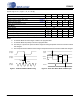
CS8416 18.2.5 Jitter Attenuation Shown in Figure 25 is the jitter attenuation plot. The AES3 and IEC60958-4 specifications state a maximum of 2 dB jitter gain or peaking. 4 2 external J itter Attenuation (dB ) 0 2 4 6 8 10 12 1 10 10 0 10 1 2 10 J itter F requency (Hz) 10 3 10 4 10 5 Figure 25.
CS8416 19.PACKAGE DIMENSIONS 28L SOIC (300 MIL BODY) PACKAGE DRAWING E H 1 b c ∝ D L SEATING PLANE A e DIM A A1 b C D E e H L ∝ A1 MIN 0.093 0.004 0.013 0.009 0.697 0.291 0.040 0.394 0.016 0° INCHES NOM 0.098 0.008 0.017 0.011 0.705 0.295 0.050 0.407 0.026 4° MAX 0.104 0.012 0.020 0.013 0.713 0.299 0.060 0.419 0.050 8° MIN 2.35 0.10 0.33 0.23 17.70 7.40 1.02 10.00 0.40 0° MILLIMETERS NOM 2.50 0.20 0.42 0.28 17.90 7.50 1.27 10.34 0.65 4° MAX 2.65 0.30 0.51 0.32 18.10 7.60 1.52 10.65 1.
CS8416 28L TSSOP (4.4 mm BODY) PACKAGE DRAWING N D E11 A2 E e b2 SIDE VIEW A ∝ A1 END VIEW L SEATING PLANE 1 2 3 TOP VIEW DIM A A1 A2 b D E E1 e L µ MIN -0.002 0.03150 0.00748 0.378 BSC 0.248 0.169 -0.020 0° INCHES NOM -0.004 0.035 0.0096 0.382 BSC 0.2519 0.1732 0.026 BSC 0.024 4° MAX 0.47 0.006 0.04 0.012 0.386 BSC 0.256 0.177 -0.029 8° MIN -0.05 0.80 0.19 9.60 BSC 6.30 4.30 -0.50 0° MILLIMETERS NOM -0.10 0.90 0.245 9.70 BSC 6.40 4.40 0.65 BSC 0.60 4° NOTE MAX 1.20 0.15 1.00 0.30 9.
CS8416 28-PIN QFN (5 × 5 MM BODY) PACKAGE DRAWING b D Pin #1 Corner e Pin #1 Corner E2 E A1 D2 L A Top View Side View Bottom View INCHES DIM A A1 b D D2 E E2 e L MIN -0.0000 0.0071 0.1220 0.1220 0.0197 NOM --0.0091 0.1969 BSC 0.1240 0.1969 BSC 0.1240 0.0197 BSC 0.0236 MILLIMETERS MAX 0.0394 0.0020 0.0118 MIN -0.00 0.18 0.1260 3.10 0.1260 3.10 0.0276 0.50 NOM --0.23 5.00 BSC 3.15 5.00 BSC 3.15 0.50 BSC 0.60 NOTE MAX 1.00 0.05 0.30 3.20 3.20 0.
CS8416 20.
CS8416 21.REVISION HISTORY Release Changes F1 -Reformatted “Features” on page 1 -Added RMCK/OMCK maximum in“Switching Characteristics” on page 8. -Corrected AES3 Direct format in “Serial Audio Output Example Formats” on page 24. -Corrected Table 2 and page 28 text referencing VCO idle frequency. -Added timing note to Figure 10 on page 32. -Corrected “Control Port Description” on page 33 to reflect the Auto-Increment function of the MAP.