
Manual

DS470F4 7
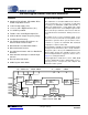
CS8415A
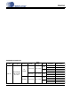
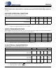
DIGITAL INPUT CHARACTERISTICS
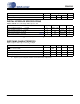
DIGITAL INTERFACE SPECIFICATIONS
AGND = DGND = 0 V; all voltages with respect to 0 V.
5. At 5.0 V mode, V
IL
= 0.8 V (Max), at 3.3 V mode, V
IL
=0.4 V (Max).
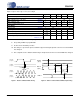
SWITCHING CHARACTERISTICS
Inputs: Logic 0 = 0 V, Logic 1 = VL+; C
L
= 20 pF.
6. Cycle-to-cycle using 32 to 96 kHz external PLL filter components.
Parameters Symbol Min Typ Max Units
Input Leakage Current
I
in
-±1±10µA
Differential Input Voltage, RXP0 to RXN0
V
TH
-200- mV
Parameters Symbol Min Max Units
High-Level Output Voltage (I
OH
= -3.2 mA)
V
OH
(VL+) - 1.0 - V
Low-Level Output Voltage (I
OH
= 3.2 mA)
V
OL
-0.4V
High-Level Input Voltage, except RX
n
V
IH
2.0 (VL+) + 0.3 V
Low-Level Input Voltage, except RX
n
(Note 5)
V
IL
-0.3 0.4/0.8 V
Parameter Symbol Min Typ Max Units
RST pin Low Pulse Width
200 - - µs
PLL Clock Recovery Sample Rate Range
8.0 - 108.0 kHz
RMCK output jitter (Note 6)
- 200 - ps RMS
RMCK output duty cycle
40 50 60 %