
Manual

DS470F4 33
CS8415A
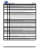
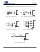
11.PIN DESCRIPTION - HARDWARE MODE
Pin Name # Pin Description
COPY
1
COPY Channel Status Bit (Output) - Reflects the state of the Copyright Channel Status bit in the incoming
AES3 data stream. If the category code is set to General, copyright will be indicated whatever the state of
the Copyright bit.
VL2+
VL+
VL3+
2
23
27
Positive Digital Power (Input) - Typically +3.3 V or +5.0 V.
EMPH
3
Pre-Emphasis (Output) - EMPH
is low when the incoming Channel Status data indicates 50/15 ms pre-
emphasis.
EMPH is high when the Channel Status data indicates no pre-emphasis or indicates pre-empha-
sis other than 50/15 ms. This pin is also a start-up option which, along with ORIG, determines the serial port
format. A 47 kΩ resistor to either VL+ or DGND is required.
RXP0
RXN0
4
5
AES3/SPDIF Receiver Port (Input) - Differential line receiver inputs for the AES3 biphase encoded data.
See Appendix A for recommended circuits.
VA+
6
Positive Analog Power (Input) - Nominally +5.0 V. This supply should be as quiet as possible since noise
on this pin will directly affect the jitter performance of the recovered clock.
AGND
7
Analog Ground (Input) - Ground for the analog circuitry in the chip. AGND and DGND should be connected
to a common ground area under the chip.
FILT
8
PLL Loop Filter (Output) - An RC network should be connected between this pin and ground. See “Appen-
dix C: PLL Filter” on page 41
for recommended schematic and component values.
RST
9
Reset (Input) - When RST is low, the CS8415A enters a low power mode and all internal states are reset.
On initial power up, RST
must be held low until the power supply is stable, and all input clocks are stable in
frequency and phase. This is particularly true in hardware mode with multiple CS8415A devices where syn-
chronization between devices is important.