
Manual

DS470F4 11
CS8415A
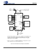
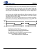
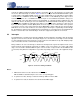
2. TYPICAL CONNECTION DIAGRAM
RXP0
RXN0
AES3/
SPDIF
Sources
Clock Control RMCK
Hardware
Control
RST
RERR
EMPH
3-wire Serial
Audio Input
Device
OLRCK
OSCLK
SDOUT
SDA/CDOUT
AD0/CS
SCL/CCLK
AD1/CDIN
U
INT
VA+ V L +
Ferrite *
Bead
+5.0 V
Analog
Supply*
0.1 Fµ
0.1 Fµ
* A separate analog supply is only necessary in applications where RMCK is used
for a jitter sensitive task. For applications where RMCK is not used for a jitter
sensitive task, connect VA+ to VD+ via a ferrite bead. Keep the decoupling
capacitor between VA+ and AGND.
DGNDFILTAGND
RFILT
CFILT CRIP
H/S
DGND2
RXP1
RXP2
RXP3
RXP4
RXP5
RXP6
CS8415A
+3.3 V or +5.0 V
Digital Supply
**
**
Please see section 5.1 "7:1 S/PDIF Input Multiplexer" and Appendix A for typical
input configurations and recommended input circuits.
A2D
/
Microcontroller
Figure 5. Recommended Connection Diagram for Software Mode