CS8415A 96 kHz Digital Audio Interface Receiver Features General Description ! Complete EIAJ CP1201, IEC-60958, AES3, The CS8415A is a monolithic CMOS device which receives and decodes one of 7 channels of audio data according to the IEC60958, S/PDIF, EIAJ CP1201, or AES3. The CS8415A has a serial digital audio output port and comprehensive control ability through a 4-wire microcontroller port. Channel status and user data are assembled in block-sized buffers, making read access easy.
CS8415A ORDERING INFORMATION Product Description Package Grade Temp Range Pb-Free YES 28TSSOP CS8415A 96 kHz Digital Audio Interface Receiver Commercial -10 to +70°C NO Industrial -40 to +85°C YES YES 28-SOIC Commercial -10 to +70°C NO CDB8415A CS8415A Evaluation Board 2 - - - Container Order Number Rail CS8415A-CZZ Tape and Reel CS8415A-CZZR Rail CS8415A-CZ Tape and Reel CS8415A-CZR Rail CS8415A-IZZ Tape and Reel CS8415A-IZZR Rail CS8415A-CSZ Tape and Reel CS8415A-CSZR Rail
CS8415A TABLE OF CONTENTS 1. CHARACTERISTICS AND SPECIFICATIONS ..................................................................................... 6 SPECIFIED OPERATING CONDITIONS .............................................................................................. 6 ABSOLUTE MAXIMUM RATINGS ........................................................................................................ 6 DC ELECTRICAL CHARACTERISTICS ......................................................................
CS8415A 13. APPENDIX A: EXTERNAL AES3/SPDIF/IEC60958 RECEIVER COMPONENTS .......................... 35 13.1 AES3 Receiver External Components ........................................................................................ 35 13.2 Isolating Transformer Requirements .......................................................................................... 36 14. APPENDIX B: CHANNEL STATUS AND USER DATA BUFFER MANAGEMENT ........................ 37 14.1 AES3 Channel Status (C) Bit Management .........
CS8415A LIST OF FIGURES Figure 1. Audio Port Master Mode Timing ................................................................................................... 8 Figure 2. Audio Port Slave Mode and Data Input Timing............................................................................. 8 Figure 3. SPI Mode Timing .......................................................................................................................... 9 Figure 4. I²C Mode Timing ....................................
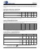
CS8415A 1. CHARACTERISTICS AND SPECIFICATIONS All Min/Max characteristics and specifications are guaranteed over the Specified Operating Conditions. Typical performance characteristics and specifications are derived from measurements taken at nominal supply voltages and TA = 25°C. SPECIFIED OPERATING CONDITIONS AGND, DGND = 0 V, all voltages with respect to 0 V. Parameter Symbol Min Typ Max Units VA+ VL+ 4.5 2.85 5.0 3.3 or 5.0 5.5 5.
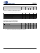
CS8415A DIGITAL INPUT CHARACTERISTICS Parameters Input Leakage Current Differential Input Voltage, RXP0 to RXN0 Symbol Min Typ Max Units Iin - ±1 ±10 µA VTH - 200 - mV DIGITAL INTERFACE SPECIFICATIONS AGND = DGND = 0 V; all voltages with respect to 0 V. Parameters Symbol Min Max Units High-Level Output Voltage (IOH = -3.2 mA) VOH (VL+) - 1.0 - V Low-Level Output Voltage (IOH = 3.2 mA) VOL - 0.4 V High-Level Input Voltage, except RXn VIH 2.0 (VL+) + 0.3 V VIL -0.3 0.4/0.
CS8415A SWITCHING CHARACTERISTICS - SERIAL AUDIO PORTS Inputs: Logic 0 = 0 V, Logic 1 = VL+; CL = 20 pF.
CS8415A SWITCHING CHARACTERISTICS - CONTROL PORT - SPI MODE Inputs: Logic 0 = 0 V, Logic 1 = VL+; CL = 20 pF. Parameter Symbol Min Typ Max Units fsck 0 - 6.0 MHz CS High Time Between Transmissions tcsh 1.
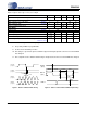
CS8415A SWITCHING CHARACTERISTICS - CONTROL PORT - I²C MODE (Note 15), Inputs: Logic 0 = 0 V, Logic 1 = VL+; CL = 20 pF. Parameter Symbol Min Typ Max Units SCL Clock Frequency fscl - - 100 kHz Bus Free Time Between Transmissions tbuf 4.7 - - µs Start Condition Hold Time (prior to first clock pulse) thdst 4.0 - - µs Clock Low Time tlow 4.7 - - µs Clock High Time thigh 4.0 - - µs Setup Time for Repeated Start Condition tsust 4.
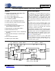
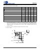
CS8415A 2. TYPICAL CONNECTION DIAGRAM +5.0 V Analog Supply* Ferrite * Bead VA+ ** AES3/ SPDIF Sources Clock Control Hardware Control +3.3 V or +5.0 V Digital Supply 0.1µF 0.
CS8415A 3. GENERAL DESCRIPTION The CS8415A is a monolithic CMOS device which receives and decodes audio data according to the AES3, IEC60958, S/PDIF, and EIAJ CP1201 interface standards. Input data is either differential or single-ended. A low-jitter clock is recovered from the incoming data using a PLL. The decoded audio data is output through a configurable, 3-wire output port.
CS8415A 4. SERIAL AUDIO OUTPUT PORT A 3-wire serial audio output port is provided. The port can be adjusted to suit the attached device setting the control registers. The following parameters are adjustable: master or slave, serial clock frequency, audio data resolution, left or right justification of the data relative to left/right clock, optional one-bit cell delay of the first data bit, the polarity of the bit clock, and the polarity of the left/right clock.
CS8415A when repeated or dropped samples occur. The CS8415A allows immediate mute of the serial audio output port audio data by the MUTESAO bit of Control Register 1.
CS8415A 5. AES3 RECEIVER The CS8415A includes an AES3 digital audio receiver. A comprehensive buffering scheme provides read access to the channel status and user data. This buffering scheme is described in Appendix B. The AES3 receiver accepts and decodes audio and digital data according to the AES3, IEC60958 (S/PDIF), and EIAJ CP-1201 interface standards.
CS8415A pulse on RERR, invoke the occurrence of a RERR interrupt, and affect the current audio sample according to the status of the HOLD bits. The HOLD bits allow a choice of holding the previous sample, replacing the current sample with zero (mute), or not changing the current audio sample.
CS8415A 5.8 Mono Mode Operation An AES3 stream may be used in more than one way to transmit 96 kHz sample rate data. One method is to double the frame rate of the current format. This results in a stereo signal with a sample rate of 96 kHz, carried over a single twisted pair cable. An alternate method is implemented using the 2 sub-frames in a 48kHz frame rate AES3 signal to carry consecutive samples of a mono signal, resulting in a 96-kHz sample rate stream.
CS8415A 6. CONTROL PORT DESCRIPTION AND TIMING The control port is used to access the registers, allowing the CS8415A to be configured for the desired operational modes and formats. In addition, Channel Status and User data may be read through the control port. The operation of the control port may be completely asynchronous with respect to the audio sample rates. However, to avoid potential interference problems, the control port pins should remain static if no operation is required.
CS8415A 6.2 I²C Mode In I²C mode, SDA is a bidirectional data line. Data is clocked into and out of the part by the clock, SCL, with the clock to data relationship as shown in Figure 9. There is no CS pin. Each individual CS8415A is given a unique address. Pins AD0 and AD1 form the two least significant bits of the chip address and should be connected to VL+ or DGND as desired. The EMPH pin is used to set the AD2 bit by connecting a resistor from the EMPH pin to VL+ or to DGND.
CS8415A 7.
CS8415A 8. CONTROL PORT REGISTER BIT DEFINITIONS 8.
CS8415A MUX2:0 - 7:1 S/PDIF Input Multiplexer Select Line Control Default = ‘000’ 000 - RXP0 001 - RXP1 010 - RXP2 011 - RXP3 100 - RXP4 101 - RXP5 110 - RXP6 111 - Reserved 8.3 Clock Source Control (04h) 7 6 5 4 3 2 1 0 0 RUN 0 0 0 0 0 0 This register configures the clock sources of various blocks. In conjunction with the Data Flow Control register, various Receiver/Transmitter/Transceiver modes may be selected.
CS8415A normally occupied by the P bit is used to indicate the location of the block start, SDOUT pin only, serial audio output port clock must be derived from the AES3 receiver recovered clock) SOJUST - Justification of SDOUT data relative to OLRCK Default = ‘0’ 0 - Left-justified 1 - Right-justified (master mode only) SODEL - Delay of SDOUT data relative to OLRCK, for left-justified data formats Default = ‘0’ 0 - MSB of SDOUT data occurs in the first OSCLK period after the OLRCK edge 1 - MSB of SDOUT data
CS8415A 8.6 Interrupt 2 Status (08h) (Read Only) 7 6 5 4 3 2 1 0 0 0 0 0 DETU 0 QCH 0 For all bits in this register, a “1” means the associated interrupt condition has occurred at least once since the register was last read. A ”0” means the associated interrupt condition has NOT occurred since the last reading of the register. Reading the register resets all bits to 0, unless the interrupt mode is set to level and the interrupt source is still true.
CS8415A 8.10 Interrupt 2 Mode MSB (0Dh) and Interrupt 2 Mode LSB (0Eh) 7 0 0 6 0 0 5 0 0 4 0 0 3 DETU1 DETU0 2 0 0 1 QCH1 QCH0 0 0 0 The two Interrupt Mode registers form a 2-bit code for each Interrupt Register 1 function. There are three ways to set the INT pin active in accordance with the interrupt condition. In the Rising edge active mode, the INT pin becomes active on the arrival of the interrupt condition.
CS8415A ORIG - SCMS generation indicator, decoded from the category code and the L bit. 0 - Received data is 1st generation or higher 1 - Received data is original Note: 8.12 COPY and ORIG will both be set to 1 if the incoming data is flagged as professional, or if the receiver is not in use. Receiver Error (10h) (Read Only) 7 6 5 4 3 2 1 0 0 QCRC CCRC UNLOCK V CONF BIP PAR This register contains the AES3 receiver and PLL status bits.
CS8415A 8.13 Receiver Error Mask (11h) 7 6 5 4 3 2 1 0 0 QCRCM CCRCM UNLOCKM VM CONFM BIPM PARM The bits in this register serve as masks for the corresponding bits of the Receiver Error Register. If a mask bit is set to 1, the error is unmasked, meaning that its occurrence will appear in the receiver error register, will affect the RERR pin, will affect the RERR interrupt, and will affect the current audio sample according to the status of the HOLD bit.
CS8415A 8.15 User Data Buffer Control (13h) 7 6 5 4 3 2 1 0 0 0 0 0 0 0 DETUI 0 DETUI - D to E U-data buffer transfer inhibit bit. Default = ‘0’ 0 - Allow U-data D to E buffer transfers 1 - Inhibit U-data D to E buffer transfers 8.
CS8415A 8.19 CS8415A I.D. and Version Register (7Fh) (Read Only) 7 6 5 4 3 2 1 0 ID3 ID2 ID1 ID0 VER3 VER2 VER1 VER0 ID3:0 - ID code for the CS8415A. Permanently set to 0100 VER3:0 - CS8415A revision level.
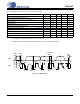
CS8415A 9. PIN DESCRIPTION - SOFTWARE MODE SDA/CDOUT AD0/CS EMPH RXP0 RXN0 VA+ AGND FILT RST RMCK RERR RXP1 RXP2 RXP3 1 2 3*+ 4* 5* 6* 7* 8* 9* 10* 11* 12 13 14 28 27 26 25 *24 *23 *22 *21 20 19 *18 *17 *16 15 SCL/CCLK AD1/CDIN RXP6 RXP5 H/S VL+ DGND OMCK U INT SDOUT OLRCK OSCLK RXP4 * Pins which remain the same function in all modes. + Pins which require a pull up or pull down resistor to select the desired startup option.
CS8415A Pin Name # Pin Description AGND 7 Analog Ground (Input) - Ground for the analog circuitry in the chip. AGND and DGND should be connected to a common ground area under the chip. FILT 8 PLL Loop Filter (Output) - An RC network should be connected between this pin and ground. See “Appendix C: PLL Filter” on page 41 for recommended schematic and component values. 9 Reset (Input) - When RST is low, the CS8415A enters a low power mode and all internal states are reset.
CS8415A 10.HARDWARE MODE The CS8415A has a hardware mode which allows using the device without a microcontroller. Hardware mode is selected by connecting the H/S pin to VL+. Various pins change function in hardware mode, described in the hardware mode pin definition section. Hardware mode data flow is shown in Figure 10. Audio data is input through the AES3 receiver, and routed to the serial audio output port. The PRO, COPY, ORIG, EMPH, and AUDIO channel status bits are output on pins.
CS8415A 11.PIN DESCRIPTION - HARDWARE MODE Pin Name # Pin Description COPY Channel Status Bit (Output) - Reflects the state of the Copyright Channel Status bit in the incoming COPY 1 AES3 data stream. If the category code is set to General, copyright will be indicated whatever the state of the Copyright bit. VL2+ VL+ VL3+ 2 23 Positive Digital Power (Input) - Typically +3.3 V or +5.0 V. 27 EMPH Pre-Emphasis (Output) - EMPH is low when the incoming Channel Status data indicates 50/15 ms preemphasis.
CS8415A Pin Name # Pin Description Recovered Master Clock (Output) - Recovered master clock output when PLL is locked to the incoming AES3 stream. Frequency is 256x the sample rate (Fs). RMCK 10 RERR 11 pin is updated once per sub-frame of incoming AES3 data. Conditions that can cause RERR to go high are: Receiver Error (Output) - When high, indicates an error condition in the AES3 receiver. The status of this validity bit high, parity error, bi-phase coding error, and loss of lock by the PLL.
CS8415A 12. APPLICATIONS 12.1 Reset, Power Down and Start-Up When RST is low, the CS8415A enters a low-power mode and all internal states are reset, including the control port and registers, and the outputs are muted. When RST is high, the control port becomes operational and the desired settings should be loaded into the control registers. Writing a 1 to the RUN bit will then cause the part to leave the low-power state and begin operation.
CS8415A 13.APPENDIX A: EXTERNAL AES3/SPDIF/IEC60958 RECEIVER COMPONENTS 13.1 AES3 Receiver External Components The CS8415A AES3 receiver is designed to accept both the professional and consumer interfaces. The digital audio specifications for professional use call for a balanced receiver, using XLR connectors, with 110 Ω ±20% impedance. The XLR connector on the receiver should have female pins with a male shell.
CS8415A 13.2 Isolating Transformer Requirements Please refer to the application note AN134: AES and SPDIF Recommended Transformers for resources on transformer selection. XLR CS8415A * See Text RXP0 110 Ω 110 Ω Twisted XLR 1 0.01 µF CS8415A RXP0 110 Ω 110 Ω Twisted RXN0 Pair * See Text 0.01 µF RXN0 Pair 1 Figure 11. Professional Input Circuit Figure 12. Transformerless Professional Input Circuit .01µF RCA Phono 75 Ω Coax 0.
CS8415A 14.APPENDIX B: CHANNEL STATUS AND USER DATA BUFFER MANAGEMENT 14.1 AES3 Channel Status (C) Bit Management The CS8415A contains sufficient RAM to store a full block of C data for both A and B channels (192 x 2 = 384 bits), and also 384 bits of U information. The user may read from these buffer RAMs through the control port. The buffering scheme involves 2 block-sized buffers, named D and E, as shown in Figure 16. The MSB of each byte represents the first bit in the serial C data stream.
CS8415A A flowchart for reading the E buffer is shown in Figure 17. Since a D-to-E interrupt just occurred after reading, there is a substantial time interval until the next D-to-E transfer (approximately 24 frames worth of time). This is usually plenty of time to access the E data without having to inhibit the next transfer. D to E interrupt occurs Optionally set D to E inhibit Read E data If set, clear D to E inhibit Return Figure 17. Flowchart for Reading the E Buffer 14.2.
CS8415A One-byte mode saves the user substantial control port access time, as it effectively accesses 2 bytes worth of information in 1 byte's worth of access time. If the control port's autoincrement addressing is used in combination with this mode, multi-byte accesses such as full-block reads can be done especially efficiently. 14.2.3.2 Two-Byte Mode There are those applications in which the A and B channel status blocks will not be the same, and the user is interested in accessing both blocks.
CS8415A 15.APPENDIX C: PLL FILTER 15.1 General An on-chip Phase Locked Loop (PLL) is used to recover the clock from the incoming data stream. Figure 18 is a simplified diagram of the PLL in these parts. When the PLL is locked to an AES3 input stream, it is updated at each preamble in the AES3 stream. This occurs at twice the sampling frequency, FS. When the PLL is locked to ILRCK, it is updated at FS so that the duty cycle of the input doesn’t affect jitter.
CS8415A 15.2 External Filter Components 15.2.1 General The PLL behavior is affected by the external filter component values. Figure 5 on page 11 shows the recommended configuration of the two capacitors and one resistor that comprise the PLL filter. In Table 6, the component values shown have the highest corner frequency jitter attenuation curve, takes the shortest time to lock, and offers the best output jitter performance.
CS8415A 15.3 Component Value Selection When transitioning from one revision of the part another, component values may need to be changed.
CS8415A 15.3.3 Jitter Tolerance Shown in Figure 20 is the Receiver Jitter Tolerance template as illustrated in the AES3 and IEC60958-4 specification. CS8415A parts used with the appropriate external PLL component values (as noted in Table 6) have been tested to pass this template. Figure 20.
CS8415A 15.3.4 Jitter Attenuation 5 5 0 0 Jitter Attenuation (dB) Jitter Attenuation (dB) Shown in Figure 21, Figure 22, Figure 23, and Figure 24 are jitter attenuation plots for the various revisions of the CS8415A when used with the appropriate external PLL component values (as noted in Table 6). The AES3 and IEC60958-4 specifications do not have allowances for locking to sample rates less than 32 kHz. These specifications state a maximum of 2 dB jitter gain or peaking.
CS8415A 16.REVISION HISTORY Release Date PP1 November 1999 1st Preliminary Release Changes PP2 November 2000 2nd Preliminary Release PP3 May 2001 3rd Preliminary Release PP4 January 2003 4th Preliminary Release F1 January 2004 Final Release Updated “Appendix C: PLL Filter” on page 41 to include information from errata ER470E2 F2 August 2004 -Added lead-free device ordering information. F3 December 2004 F4 August 2005 -Changed format of Figure 6 on page 14.