
Manual

4 DS134PP2-B
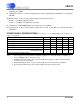
DIGITAL PIN CHARACTERISTICS (T
A
= 25 °C; Supply= 3.0 V)
SPEC TABLE TITLE (INSERT 5 COLUMN TABLE) Spec Table Condition
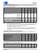
Notes: 9. 20% duty cycle, max pulse width 19.5 µs (3/16 of (1/9600 bps)).
ABSOLUTE MAXIMUM RATINGS (All voltages with respect to 0 V)
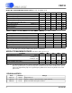
Notes: 10. In normal oscillator mode, the crystal is internally loaded with 20 pF, which is the standard loading at
which the crystal frequency is tuned. In low power oscillator mode, the internal loading on the crystal is
reduced to approximately 5 pF. The crystal frequency will therefore increase by about 0.03% in low
power mode.
For pricing, delivery, and technical assistance, call (512) 445-7222.
Parameter Symbol Min Typ Max Unit
High-level Input Voltage V
IH
2.0 - - V
Low-level Input Voltage V
IL
--0.8V
High-level Output Voltage V
OH
VD - 0.3 - - V
Low-level Output Voltage V
OL
--0.3V
Output Leakage Current in Hi-Z state - - 0.2 µA
Input Leakage Current (Digital Inputs) - - 0.2 µA
Output Capacitance C
OUT
-5-pF
Input Capacitance C
IN
-5-pF
Parameter Symbol Min Max Unit
Power Supplies -0.3 6.0 V
Input Current Except Supply Pins & Driver Pins - ±10 mA
Input Voltage -0.3 VD + 0.3 V
LED Output Current (each driver) (Note 9) - 750 mA
Ambient Temperature (Power Applied) -55 +125 °C
Storage Termperature -65 +150 °C
ESD using humand body model (100 pF with series 1.5 k
Ω
) 2000 - V
Parameter Symbol Min Typ Max Unit
XTALIN/EXTCLK frequencies (Note )
CLKFR pin low
CLKFR pin high
-
-
3.6864
1.8432
-
-
MHz
MHz
EXTCLK duty cycle (as an input) 45 50 55 %
Crystal Oscillator start up time - - 25 ms
CS8130
4 DS134F1-B
CS8130
4 DS134F1-B1
REVISION HISTORY
Date Revision Change
NOV ‘97 PP2-B Original Release
SEP ‘05 F1-B Update company contact information, legal statement.
MAR ‘06 F1-B1 Remove invalid contact phone number.
CS8130
4 DS134F1-B1
CS8130
4 DS134F1-B1
CS8130
4 DS134F1-B1