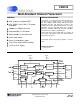
CS8130 CS8130 Semiconductor Corporation Multi-Standard Infrared Transceiver Features General Description • Adds IR port to standard UART • IrDA, HPSIR, ASK (CW) & TV remote The CS8130 is an infrared transceiver integrated circuit. The receive channel includes on-chip high gain PIN diode amplifier, IrDA, HPSIR, ASK & TV remote compatible decoder, and data pulse stretcher. The transmit path includes IrDA, HPSIR, ASK & TV remote compatible encoder, and LED driver.
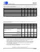
CS8130 CS8130 TRANSMITTER DRIVER CHARACTERISTICS (TA = 25 °C; All V+ = 3.0V, Digital Input Levels: Logic 0 = 0V, Logic 1 = V+; unless otherwise specified) Parameter Symbol Output capacitance (Note 1) Output rise time (10% to 90%) tr Output fall time (90% to 10%) tf Overshoot over final current On resistance Off leakage current Output current (each driver) (Note 2) Output jitter relative a jitter free input clock Notes: 1. Typical LED junction capacitance is 20pF. 2.
CS8130 CS8130 POWER SUPPLY SPECIFICATIONS (TA = 25°C; V+ = 3.0V, Digital Input Levels: Logic 0 = 0V, Logic 1 = V+, Note 7) Parameter Symbol Min Typ Max Units Power Supply Voltage 2.7 3.0 5.5 V Power Supply Current - All functions enabled (Note 8) 2.5 mA Power Supply Current - All functions disabled (Note 9) 1 µA Power Supply Current - Receiver only enabled (Note 8) 2.5 mA Power Supply Current - Transmit only enabled (Note 10) 0.5 mA Oscillator Power Supply Current low power mode: 0.
CS8130 CS8130 ABSOLUTE MAXIMUM RATINGS (All voltages with respect to 0V) Parameter Symbol Min Power Supplies -0.3 Input Current Except Supply Pins & Driver Pins Input Voltage -0.3 Ambient temperature (Power Applied) -55 Storage Temperature -65 2000 ESD using human body model (100pF with series 1.5kΩ) Warning: Operation beyond these limits may result in permanent damage to the device. Normal operation is not guaranteed at these extremes. Max Units 6.0 ±10 VD+0.
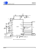
CS8130 CS8130 Ferrite Bead 10 Ω +3.0V supply + 0.1 µF To LED 0.1 µF VA+ 10 µF TGND1, 2 VD+ AGND PINC RXD RxD PINA FORM/BSY EXTCLK CTS PIN Diode + Supply LED2 LED1 XTALIN 47 µF + CS8130 XTALOUT R1 TBD Ω 3.6864 MHz or 1.8432 MHz. Can also use an external clock at 3.6864 MHz or 1.8432 MHz UART TXD TxD D/C DTR LED1C R2 TBD Ω RTS LED2C Use: LED1/R1 or:LED1/R1 & R2 or: LED1/R1 & LED2/R2 RESET TGND1 TGND2 For 2 LED, +5V supply systems, connect 2 LEDs in series.
CS8130 CS8130 OVERVIEW The CS8130 is an infrared transceiver I.C. The receive channel includes on-chip high gain PIN diode amplifier, IrDA, HP-SIR, 500 kHz Amplitu de Shift Keyin g (ASK) & TV remote compatible decoder, and data pulse stretcher. The transmit path includes IrDA, HPSIR, 500 kHz ASK & TV remote compatible encoder, and LED drivers. The computer data port is standard UART TxD and RxD compatible, and operates from 1200 to 115200 baud. An on-chip baud rate generator is provided.
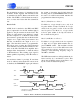
CS8130 CS8130 1 0 1 TXD TRANSMITTER On Off * LED Output B Light No Light PIN Input RECEIVER ** RXD A: 1/baud rate B: 3/16 of 1/115200 or 3/16 of A (selectable) C: 3/16 of 1/115200 to 3/16 of A C * LED1C and LED2C go low to turn on LED. ** RXD output is delayed from the PIN diode input by A (1 bit). A Figure 2.
CS8130 CS8130 then the RXD pin will oscillate at the carrier frequency. Transmit Path Data for transmission is input to the CS8130 on the TXD pin. The selected modulation scheme is then applied to the data, and the resulting signals are used to drive the LED. There are 2 LED output pins: LED1C and LED2C. They are open drain outputs, which pull down to TGND or float. The LED is connected via resistors to both LED1C and LED2C. The current level flowing through the LED is determined by the external resistors.
CS8130 CS8130 The modulation frequency is determined by the modulator divider registers. The transmit bit rate is determined by the TV Remote transmit bit rate divider. The UART to CS8130 baud rate must be set to at least 20% faster than the transmit bit rate. the format of incoming data. If high, then the incoming data is in IrDA/HPSIR format. If low, the data is in ASK format which matches the programmed modulation frequency.
CS8130 CS8130 Mode 3 (TV remote) Receive Choices ing register to a rate which is less than 80% of the UART baud rate. The CS8130 will now start sampling the demodulated infrared data at the TV remote receive sample rate. The stream of samples will be assembled into characters, with a start bit and a stop bit, and will be transmitted to the UART via RXD at the UART baud rate. The system software can then concatenate successive characters and reconstruct the incoming bit stream.
CS8130 CS8130 then switch to "programmed T period" mode to reduce processing overhead in the host CPU. external clock, then RESET low can be short (>1 µs). Clock Generation Power Down The primary clock required is 3.6864 MHz. This may be generated by attaching a 3.6864 MHz crystal to the XTALIN and XTALOUT pins. In this case, the EXTCLK pin becomes an output, and may be used to drive external devices. If this is not required, power may be saved by disabling the EXTCLK output.
CS8130 CS8130 Reset register is always accessible, independent of the state of the shadow bit. The shadow bit must be written to 0 to enable access to registers 0 through 15. Bringing the RESET pin low will force the internal logic, including the control registers, into a known state, provided the PWRDN pin is high. RESET is disabled if the PWRDN pin is low. The reset state is given in each register definition table.
CS8130 CS8130 Control Data Byte Format BIT D7 D6 D5 D4 D3 D2 D1 D0 AD3 AD2 AD1 AD0 CD3 CD2 CD1 CD0 NAME AD3-0 Register Address (4 bits of transmitted address + MSB, which is the shadow (SHDW) bit state [Control Reg #3]. All registers have 4 data bits).
CS8130 CS8130 Register 0, Control Register #1 D3 D2 D1 D0 Register ECHO 0 RXEN TXEN Reset (R) 0 0 0 0 BIT ECHO RXEN NAME Echo Control Characters Receiver Enable TXEN Transmitter Enable VALUE 0 1 0 1 0 1 FUNCTION R Do not echo control characters Echo control characters.
CS8130 CS8130 Register 2, Transmit Mode Register #1 D3 D2 D1 Register DIR TVR PWID Reset (R) 0 0 0 BIT DIR NAME Direct Mode Enable TVR TV Remote Mode Enable Select Pulse Width PWID MODU D0 MODU 0 VALUE 0 1 0 1 0 1 0 1 Select Modulation Method R R R R FUNCTION Mode 4 Direct access mode disabled Mode 4 Direct access mode enabled Mode 3 TV remote mode disabled Mode 3 TV remote mode enabled Set pulse width to 1.
CS8130 CS8130 Register 5, Receive Mode Register D3 Register Reset (R) BIT RTVR, RMOD, RWIDS, RWIDL D2 D1 D0 RTVR RMOD RWIDS RWIDL 0 0 1 1 NAME Receive Mode VALUE 0000 0001 0010 0011 0100 1000 1100 FUNCTION 0 Mode 2 Amplitude modulated carrier mode 1 Mode 1a IRDA - fixed 1.6µs pulse 2 Mode 1b IRDA - variable 3/16 bit cell time pulse 3 R Mode 1c IRDA - Any width pulse from 1.
CS8130 CS8130 Register 8, Baud Rate Divider Register #1 D3 D2 D1 D0 Register BR3 BR2 BR1 BR0 Reset (R) 0 1 1 1 Register 9, Baud Rate Divider Register #2 D3 D2 D1 D0 Register BR7 BR6 BR5 BR4 Reset (R) 0 0 0 1 BIT BR7-0 NAME Baud Rate Divider Value (BRD). BRD=(3.6864E6/ (16*BR))-1, where BRD = divider value and BR = desired baud rate. VALUE 01011111 00101111 00010111 00001011 00001001 00000010 00000001 FUNCTION 95 2400 bps 47 4800 bps 23 R 9600 bps 11 19.2 kbps 5 38.
CS8130 CS8130 Register 12, Output Pin Control Register D3 Register Reset (R) BIT RXDT RXDH FORT FORH D2 RXDT RXDH 0 1 D1 FORT 0 D0 FORH 1 NAME RXD output pin three-state enable RXD output pin high/low enable FORM/BSY output pin three-state enable FORM/BSY output pin high/low enable VALUE 0 1 0 1 0 1 R In In In R In R In In 0 1 In power down, FORM/BSY will go low, if FORT = 0 R In power down, FORM/BSY will go high, if FORT = 0 VALUE 0 1 FUNCTION R Enable access to registers 0 though 15 Enabl
CS8130 CS8130 Register 16, TV Remote Receive Timing Register #1 D3 Register Reset (R) D2 D1 TVR3 TVR2 TVR1 1 1 1 D0 TVR0 1 Register 17, TV Remote Receive Timing Register #2 D3 D2 Register TVR7 TVR6 Reset (R) 1 1 D1 TVR5 1 D0 TVR4 1 Register 18, TV Remote Receive Timing Register #3 D3 Register Reset (R) BIT TVR11-0 D2 TVR11 TVR10 0 1 D1 TVR9 1 NAME TV remote mode receiver timing register TVR = (3.6864E6 * T) -1 where T = the incoming bit period, and TVR = this register value.
CS8130 CS8130 Register 19, TV Remote Transmit Bit Rate Divider Register #1 D3 Register Reset (R) D2 D1 TBR3 TBR2 TBR1 1 1 1 D0 TBR0 1 Register 20, TV Remote Transmit Bit Rate Divider Register #2 D3 D2 Register TBR7 TBR6 Reset (R) 0 1 BIT TBR7-0 D1 D0 TBR5 1 TBR4 1 NAME TV remote mode transmit bit rate register TBR= (3.6864E6/(16*RATE)) -1 where TBR is this register value & RATE is the desired transmit bit rate.
CS8130 CS8130 Register 24, Receive ASK Timing Sensitivity Register D3 Register Reset (R) BIT RAT3-0 D2 D1 RAT3 RAT2 RAT1 0 0 0 D0 RAT0 0 NAME Receiver ASK Timing Sensitivity. Timing window = +0.27 µs to -RAT(2/3.6864E06) - 0.27 µs VALUE 0000 0001 0010 ↓ 1111 0 R +0.27 1 +0.27 2 +0.27 ↓ 15 +0.27 FUNCTION µs to -0.27 µs window (500 kHz ASK mode) µs to -0.54 - 0.27 µs window µs to -1.08 - 0.27 µs window ↓ µs to -8.14 - 0.
CS8130 CS8130 Grounding & Layout Optical Components Grounding and layout for the CS8130 are critical, because of the sensitive nature of the PIN diode amplifier. The CS8130 should be over its own dedicated ground plane. The PIN diode should be very close to the PINA and PINC pins. The PIN diode traces should be very short (< 5 mm), and should be surrounded by ground plane. There should be holes in the ground plane provided for mounting a metal shield over the CS8130 and the PIN diode for EMI shielding.
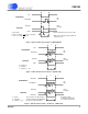
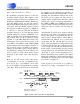
CS8130 CS8130 10 Ω 10 µF + 0.1 µF 5 7 BPV23NF 8 12 VA+ VD+ AGND PINA +3V RESET CS8130 RXD FORM/BSY 5.2 Ω (2) 5.2 Ω (2) 1 4 17 3.6864 MHz PINC 47 µF Notes: (1) This circuit has not yet been built and debugged. (2) Choice of LED, power consumption and physical positioning will affect R value. EXTCLK XTALOUT 6 +3V 10 µF 19 XTALIN TSHA5502 + + 0.1 µF TXD LED1C D/C LED2C PWRDN CLKFR 18 11 13 16 14 15 10 9 TGND1 TGND2 DGND 2 3 20 +3V 0.33 µF 1 5 0.33 µF CIA- EN 2 CIA+ 4 0.
CS8130 CS8130 10 Ω 10 µF + 0.1 µF 5 7 BPV23NF 8 12 VA+ VD+ AGND EXTCLK PINC TSHA5502 PINA XTALIN 47 µF 5.5 Ω (2) 5.5 Ω (2) 1 4 LED1C +3V 0.33 µF 5 19 0.33 µF VCC CIB- CIA- XTALOUT 17 C2+ 18 C2- 13 11 T1IN 12 T2IN 6 R1OUT 7 R2OUT 8 R3OUT 16 FORM/BSY 14 TXD 15 D/C 11 RESET LED2C PWRDN CLKFR 10 +3V +3V 9 14 MAX562 EN Notes: (1) This circuit has not yet been built and debugged. (2) Choice of LED, power consumption and physical positioning will affect R value.
CS8130 CS8130 LED1 CATHODE TRANSMIT GROUND 1 TRANSMIT GROUND 2 LED2 CATHODE ANALOG GROUND PIN DIODE ANODE PIN DIODE CATHODE ANALOG SUPPLY CLOCK FREQUENCY POWER DOWN LED1C TGND1 TGND2 LED2C AGND PINA PINC VA+ CLKFR PWRDN 1 2 3 4 5 6 7 8 9 10 20 19 18 17 16 15 14 13 12 11 DGND EXTCLK XTALOUT XTALIN FORM/BSY D/C TXD RXD VD+ RESET DIGITAL GROUND EXTERNAL CLOCK CRYSTAL OUTPUT CRYSTAL INPUT FORMAT/BUSY DATA/CONTROL TRANSMIT DATA RECEIVE DATA DIGITAL SUPPLY RESET Power Supplies VD+ - Digital Positive Supply
CS8130 CS8130 Digital Pins RXD - Receiver Data Output Receiver output data. Normally connected to RxD on the UART. TXD - Transmit Data Input Transmitter input data. Normally connected to TxD on the UART. D/C - Data/Control Mode Input The D/C pin determines whether the input data on TXD is treated as data to be transmitted via the LED, or as control information to set up the CS8130 internal registers. The D/C pin also can act as a power down control.
CS8130 20 PIN SSOP 28 PIN SSOP N E SSOP Package Dimensions 1 2 3 TOP VIEW D1 E 11 A2 e A A1 b2 L Seating Plane END VIEW SIDE VIEW INCHES MILLIMETERS Notes: 1. "D" and "E 1 " are reference datums and do not include mold flash or protrusions, but do include mold mismatch and are measured at the parting line, mold flash or protrusions shall not exceed 0.20mm per side. 2. Dimension b does not include dambar protrusion/intrusion. Allowable dambar protrusion shall be 0.
CS8130 ORDERING INFORMATION Model Package CS8130-CS Temperature 20-pin SSOIC 0 to +70 °C ENVIRONMENTAL, MANUFACTURING, & HANDLING INFORMATION Model Number Peak Reflow Temp CS8130-CS 240 °C MSL Rating* 2 Max Floor Life 365 Days * MSL (Moisture Sensitivity Level) as specified by IPC/JEDEC J-STD-020. REVISION HISTORY Revision Date Changes PP2 JUN 1994 Initial Release F1 SEP 2005 Updated device ordering info. Updated legal notice. Added MSL data..