
User guide

CS6422
13
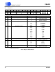
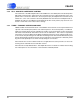
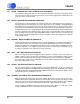
STROBE pulses must be applied to latch the data
into the CS6422.
Since the MCR is a shift register, the STROBE can
be run arbitrarily slowly with a duty cycle limited
only by the minimum high and low time specified
in “Switching Characteristics”. The Microcontrol-
ler Interface is polled at 125 µs intervals, so regis-
ter writes must be spaced at least 125 µs apart or
the register contents may be overwritten.
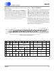
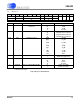
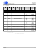
3.2.2 Register Definitions
The six control registers accessible through the
MCR are described in detail in the following tables.
These registers are addressed by bits b3-0 of the
MCR. Bit ‘b0’ must always be ‘0’. Table 2 shows
the register map with the default settings. Tables 3
through 8 show the control registers in more detail.
The Register Map at the top of each register de-
scription shows the names of all the bits, with their
reset values below the bitfield name. The reset val-
ue can also be found in the Word column of the bit-
field summary as indicated by an ‘*’.
# b15 b14 b13 b12 b11 b10 b9 b8 b7 b6 b5 b4 b3-0
0Mic
1
HDD
0
GB
10
RVol
0100
TSD
0
ACC
00
TSMde
0
0000
1 THDet
00
Taps
10
TVol
1010
RSD
0
NCC
00
AuNECD
0
0010
2 RHDet
00
RSThd
00
NseRmp
00
HDly
00
HHold
0
TDSRmp
0
RDSRmp
0
IdlTx
0
0100
3TSAtt
00
PCSen
0
TDbtS
000
RDbtS
00
TSThd
00
TSBias
00
0110
4AErle
00
AFNse
00
NErle
00
NFNse
00
RGain
00
TGain
00
1000
5HwlD
0
TD
0
APCD
0
NPCD
0
APFD
0
NPFD
0
AECD
0
NECD
0
ASdt
00
NSdt
00
1010
Table 2. MCR Control Register Mapping
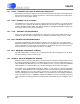
Bit15
Bit14 Bit13 Bit12
Bit11 Bit10 Bit9 Bit8
Bit7 Bit6
Bit5 Bit4 Bit3
Bit2
Bit1
Bit0DATA
DRDY
STROBE
four extra strobe pulses
12
3
4
Figure 7. Microcontroller Interface
CS6422
DS295F1 13