
Instruction Manual

CS61884
56 DS485F3
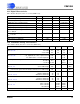
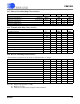
19.5 Receiver Analog Characteristics
(TA = -40°C to 85°C; TV+, RV+ = 3.3 V ±5%; GND = 0 V))
Notes: 11. Parameters guaranteed by design and characterization.
12. Using components on the CDB61884 evaluation board in Internal Match Impedance Mode.
13. Return loss = 20log10 ABS((Z1 + Z0) / (Z1 - Z0)) where Z1 - impedance of the transmitter or receiver,
and Z0 = cable impedance.
14. Assuming that jitter free clock is input to TCLK.
15. Jitter tolerance for 0 dB for T1/J1 input signal levels and 6 dB for E1 input signal levels. Jitter tolerance
increases at lower frequencies. HDB3/B8ZS coders enabled.
16. In Data Recovery Mode.
17. Jitter Attenuator in the receive path.
Parameter Min. Typ Max Units
Allowable Cable Attenuation @ 1024kHz and 772kHz - - - 12 dB
RTIP/RRING Input Impedance T1/J1 100 Ω Load
(Internal Line matching mode) E1 120Ω Load
Note 11 E1 75Ω Load
-
-
-
140
14k
50
-
-
-
Ω
RTIP/RRING Input Impedance T1/J1 100 Ω Load
(External Line matching mode) E1 120Ω Load
Note 11 E1 75Ω Load
-
-
-
14K
14k
14K
-
-
-
Ω
Receiver Dynamic Range 0.5 - - Vp
Signal to Noise margin (Per G.703, O151 @ 6dB cable Atten). Note 11 -- 18- dB
Receiver Squelch Level - 150 - mV
LOS Threshold - 200 - mV
LOS Hysteresis - 50 - mV
Data Decision Threshold E1 Modes
Note 11
41 50 59 % of
peak
Data Decision Threshold T1/J1 Modes
Note 11
56 65 74 % of
peak
Input Jitter Tolerance - E1 1 Hz - 1.8 Hz
Notes 11, 15, 17 20 Hz - 2.4 kHz
18 kHz - 100 kHz
18
1.5
0.2
-
-
-
-
-
-
UI
Input Jitter Tolerance - T1/J1 0.1 Hz - 1 Hz
Notes 11, 15, 17 4.9Hz - 300kHz
10kHz - 100 kHz
138
28
0.4
-
-
-
-
-
-
UI
Input Return Loss - E1/T1/J1 51 kHz - 102 kHz
102 kHz - 2048 kHz
Notes 11, 12, 13 2048 kHz - 3072 kHz
- 18
- 18
- 18
- 28
- 30
- 27
-
-
-
dB