
Instruction Manual
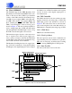
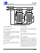

CS61884
DS485F3 41
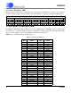
14.27 AWG Overflow Interrupt Enable Register (1Ah)
14.28 AWG Overflow Interrupt Status Register (1Bh)
14.29 Reserved Register (1Ch)
14.30 Reserved Register (1Dh)
14.31 Bits Clock Enable Register (1Eh)
14.32 Reserved Register (1Fh)
BIT NAME Description
[7:0] AWGE 7-0
This register enables changes in the overflow status to be reflected in the AWG Interrupt Sta-
tus register, thus causing as interrupt on the INT
pin. Interrupts are maskable on a per-chan-
nel basis. Register bits default to 00h after power-up or reset.
BIT NAME Description
[7:0] AWGI 7-0
The bits in this register indicate a change in status since the last AWG overflow interrupt. An
AWG overflow occurs when invalid phase data are entered, such that a sample-by-sample
addition of UI0 and UI1 results in values that exceed the arithmetic range of the 7-bit repre-
sentation. Reading this register clears the interrupt, which deactivates the INT
pin. Register
bits default to 00h after power-up or reset.
BIT NAME Description
[7:0] RSVD 7-0 RESERVED (These bits must be set to zero.)
BIT NAME Description
[7:0] RSVD 7-0 RESERVED (These bits must be set to zero.)
BIT NAME Description
[7:0] BITS 7-0 Setting a “1” to bit n in this register changes channel n to a stand-alone timing recovery unit
used for G.703 clock recovery. (Refer to BUILDING INTEGRATED TIMING SYSTEMS
(BITS) CLOCK MODE (See Section 8 on page 23) for a better description of the G.703 clock
recovery function). Register bits default to 00h after power-up or reset.
BIT NAME Description
[7:0] RSVD 7-0 RESERVED (These bits must be set to zero.)