
Instruction Manual


CS61884
12 DS485F3
WR/DS/SDI/LEN0 84 J14 I
Data Strobe/ Write Enable/Serial Data/Line Length Input
Intel Parallel Host Mode
- This pin “WR” functions as a
write enable.
Motorola Parallel Host Mode
- This pin “DS“ functions as
a data strobe input.
Serial Host Mode
- This pin “SDI” functions as the serial
data input.
Hardware Mode
- As LEN0, this pin controls the transmit
pulse shapes for both E1 and T1/J1 modes. This pin also
selects which mode is used E1 or T1/J1 (Refer to Table 5
on page 25).
RD
/RW/LEN1 85 J13 I
Read/Write/ Read Enable/Line Length Input
Intel Parallel Host Mode
- This pin “RD” functions as a
read enable.
Motorola Parallel Host Mode
- This pin “R/W” functions as
the read/write input signal.
Hardware Mode
- As LEN1, this pin controls the transmit
pulse shapes for both E1 and T1/J1 modes. This pin also
selects which mode is used E1 or T1/J1 (Refer to Table 5
on page 25).
ALE/AS
/SCLK/LE
N2
86 J12 I
Address Latch Enable/Serial Clock/Address Strobe/Line
Length Input
Intel Parallel Host Mode
- This pin “ALE” functions as the
Address Latch Enable when configured for multiplexed ad-
dress/data operation.
Motorola Parallel Host Mode
- This pin “AS” functions as
the active “low” address strobe when configured for multi-
plexed address/data operation.
Serial Host Mode
- This pin “SCLK” is the serial clock
used for data I/O on SDI and SDO.
Hardware Mode
- As LEN2, this pin controls the transmit
pulse shapes for both E1 and T1/J1 modes. This pin also
selects which mode is used E1 or T1/J1 (Refer to Table 5
on page 25).
CS
/JASEL 87 J11 I
Chip Select Input/Jitter Attenuator Select
Host Mode
- This active low input is used to enable ac-
cesses to the microprocessor interface in either serial or
parallel mode.
Hardware Mode
- This pin controls the position of the Jitter
Attenuator.
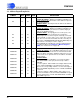
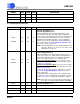
SYMBOL LQFP LFBGA TYPE DESCRIPTION
Pin State Jitter Attenuation Position
LOW Transmit Path
HIGH Receive Path
OPEN Disabled