CS61884 Octal T1/E1/J1 Line Interface Unit Features Description The CS61884 is a full-featured octal E1/T1/J1 short-haul LIU that supports both 1.544 Mbps or 2.048 Mbps data transmission. Each channel provides crystal-less jitter attenuation that complies with the most stringent standards. Each channel also provides internal AMI/B8ZS/HDB3 encoding/decoding. To support enhanced system diagnostics, channel zero can be configured for G.
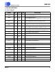
CS61884 TABLE OF CONTENTS 1. PINOUT - LQFP ........................................................................................................................................ 7 2. PINOUT - LFBGA ...................................................................................................................................... 8 3. PIN DESCRIPTIONS ................................................................................................................................. 9 3.1 Power Supplies ....
CS61884 11. 12. 13. 14. 15. 16. 10.5 Loss-of-Signal (LOS) .......................................................................................................................27 10.6 Alarm Indication Signal (AIS) ..........................................................................................................28 JITTER ATTENUATOR .........................................................................................................................28 OPERATIONAL SUMMARY .....................
CS61884 17. 18. 19. 20. 21. 22. 23. 24. 25. 4 16.1.2 Test-Logic-Reset ................................................................................................................... 45 16.1.3 Run-Test-Idle ........................................................................................................................ 45 16.1.4 Select-DR-Scan .................................................................................................................... 46 16.1.5 Capture-DR .............
CS61884 LIST OF FIGURES Figure 1. CS61884 144-LQFP Pinout ................................................................................................ 7 Figure 2. CS61884 160-Ball LFBGA Pinout ..................................................................................... 8 Figure 3. G.703 BITS Clock Mode in NRZ Mode .......................................................................... 23 Figure 4. G.703 BITS Clock Mode in RZ Mode ..............................................................
CS61884 LIST OF TABLES Table 1. Operation Mode Selection ................................................................................................. 10 Table 2. Mux/Bits Clock Selection .................................................................................................. 11 Table 3. Cable Impedance Selection ................................................................................................ 15 Table 4. G.772 Address Selection ..................................................
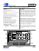
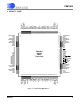
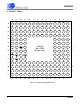
CS61884 144 143 142 141 140 139 138 137 136 135 134 133 132 131 130 129 128 127 126 125 124 123 122 121 120 119 118 117 116 115 114 113 112 111 110 109 TNEG7/UBS7 RCLK7 RPOS7/RDATA7 RNEG7/BPV7 LOS7 RTIP7 RRING7 TV+7 TTIP7 TRING7 TGND7 RRING6 RTIP6 TGND6 TRING6 TTIP6 TV+6 RTIP5 RRING5 TV+5 TTIP5 TRING5 TGND5 RRING4 RTIP4 TGND4 TRING4 TTIP4 TV+4 CLKE TXOE LOS4 RNEG4/BPV4 RPOS4/RDATA4 RCLK4 TNEG4/UBS4 1.
CS61884 2.
CS61884 3. PIN DESCRIPTIONS 3.1 Power Supplies SYMBOL LQFP LFBGA VCCIO 17 92 G1 G14 Power Supply, Digital Interface: Power supply for digital interface pins; typically 3.3V. GNDIO 18 91 G4 G11 Ground, Digital Interface: Power supply ground for the digital interface; typically 0 Volts RV0+ RV1+ 19 90 H1 H14 Power Supply, Core Circuitry: Power supply for all sub-circuits except the transmit driver; typically +3.
CS61884 3.2 Control SYMBOL MCLK LQFP 10 LFBGA E1 TYPE DESCRIPTION I Master Clock Input This pin is a free running reference clock that should be either 1.544 MHz for T1/J1 or 2.048 MHz for E1 operation. This timing reference is used as follows: - Timing reference for the clock recovery and jitter attenuation circuitry.
CS61884 SYMBOL MUX/BITSEN0 LQFP 43 LFBGA K2 TYPE I DESCRIPTION Multiplexed Interface/Bits Clock Select Host Mode -This pin configures the microprocessor interface for multiplexed or non-multiplexed operation. Hardware mode - This pin is used to enable channel 0 as a G.703 BITS Clock recovery channel (Refer to BUILDING INTEGRATED TIMING SYSTEMS (BITS) CLOCK MODE (See Section 8 on page 23). Channel 1 through 7 are not affected by this pin during hardware mode. During host mode the G.
CS61884 SYMBOL WR/DS/SDI/LEN0 RD/RW/LEN1 ALE/AS/SCLK/LE N2 CS/JASEL LQFP 84 85 86 87 LFBGA J14 J13 J12 J11 TYPE DESCRIPTION I Data Strobe/ Write Enable/Serial Data/Line Length Input Intel Parallel Host Mode - This pin “WR” functions as a write enable. Motorola Parallel Host Mode - This pin “DS“ functions as a data strobe input. Serial Host Mode - This pin “SDI” functions as the serial data input.
CS61884 SYMBOL INTL/MOT/CODE N TXOE CLKE DS485F3 LQFP 88 114 115 LFBGA H12 E14 E13 TYPE DESCRIPTION I Motorola/Intel/Coder Mode Select Input Parallel Host Mode - When this pin is “Low” the microprocessor interface is configured for operation with Motorola processors. When this pin is “High” the microprocessor interface is configured for operation with Intel processors.
CS61884 3.3 Address Inputs/Loopbacks SYMBOL A4 14 LQFP 12 LFBGA F4 TYPE DESCRIPTION I Address Selector Input Parallel Host Mode - During non-multiplexed parallel host mode operation, this pin function as the address 4 input for the parallel interface. Hardware Mode - The A4 pin must be tied low at all times.
CS61884 3.4 Cable Select SYMBOL LQFP LFBGA TYPE DESCRIPTION Cable Impedance Select Host Mode - The input voltage to this pin does not effect normal operation. Hardware Mode - This pin is used in combination with the LEN control pins (Refer to Table 5, “Hardware Mode Line Length Configuration Selection,” on page 25) to set the line impedance for all eight receivers and transmitters.
CS61884 3.6 Digital Rx/Tx Data I/O SYMBOL LQFP LFBGA TYPE DESCRIPTION Transmit Clock Input Port 0 - When TCLK is active, the TPOS and TNEG pins function as NRZ inputs that are sampled on the falling edge of TCLK. - If MCLK is active, TAOS will be generated when TCLK is held High for 16 MCLK cycles. TCLK0 36 N1 I NOTE: MCLK is used as the timing reference during TAOS and must have the appropriate stability.
CS61884 SYMBOL RCLK0 LQFP 39 LFBGA P1 TYPE DESCRIPTION O Receive Clock Output Port 0 - When MCLK is active, this pin outputs the recovered clock from the signal input on RTIP and RRING. In the event of LOS, the RCLK output transitions from the recovered clock to MCLK. - If MCLK is held “High”, the clock recovery circuitry is disabled and the RCLK output is driven by the XOR of RNEG and RPOS. - If MCLK is held “Low”, this output is in a high-impedance state.
CS61884 18 SYMBOL LQFP LFBGA TYPE DESCRIPTION RCLK2 78 M14 O Receive Clock Output Port 2 RPOS2/RDATA2 77 M13 O Receive Positive Pulse/ Receive Data Output Port 2 RNEG2/BPV2 76 M12 O Receive Negative Pulse/Bipolar Violation Output Port 2 TCLK3 74 N14 I Transmit Clock Input Port 3 TPOS3/TDATA3 73 N13 I Transmit Positive Pulse/Transmit Data Input Port 3 TNEG3/UBS3 72 N12 I Transmit Negative Pulse/Unipolar-Bipolar Select Port 3 RCLK3 71 P14 O Receive Clock Output Port 3
CS61884 SYMBOL LQFP LFBGA TYPE DESCRIPTION RCLK7 143 A1 O Receive Clock Output Port 7 RPOS7/RDATA7 142 A2 O Receive Positive Pulse/ Receive Data Output Port 7 RNEG7/BPV7 141 A3 O Receive Negative Pulse/Bipolar Violation Output Port 7 TYPE DESCRIPTION 3.7 Analog RX/TX Data I/O SYMBOL LQFP LFBGA TTIP0 45 N5 O TRING0 46 P5 O Transmit Tip Output Port 0 Transmit Ring Output Port 0 TTIP and TRING pins are the differential outputs of the transmit driver.
CS61884 20 SYMBOL LQFP LFBGA TYPE DESCRIPTION TTIP2 57 L10 O Transmit Tip Output Port 2 TRING2 58 M10 O Transmit Ring Output Port 2 RTIP2 60 M8 I Receive Tip Input Port 2 RRING2 61 L8 I Receive Ring Input Port 2 TTIP3 64 N10 O Transmit Tip Output Port 3 TRING3 63 P10 O Transmit Ring Output Port 3 RTIP3 67 P8 I Receive Tip Input Port 3 RRING3 66 N8 I Receive Ring Input Port 3 TTIP4 117 B10 O Transmit Tip Output Port 4 TRING4 118 A10 O Transmit Ring Outp
CS61884 3.8 JTAG Test Interface SYMBOL LQFP LFBGA TYPE TRST 95 G12 I TMS 96 F11 I TCK 97 F14 I TDO 98 F13 O TDI 99 F12 I SYMBOL LQFP LFBGA TYPE REF 94 H13 I DESCRIPTION JTAG Reset This active Low input resets the JTAG controller. This input is pulled up internally and may be left as a NC when not used. JTAG Test Mode Select Input This input enables the JTAG serial port when active High. This input is sampled on the rising edge of TCK.
CS61884 4. OPERATION 7. G.772 MONITORING The CS61884 is a full featured line interface unit for up to eight E1/T1/J1 lines. The device provides an interface to twisted pair or co-axial media. A matched impedance technique is employed that reduces power and eliminates the need for matching resistors. As a result, the device can interface directly to the line through a transformer without the need for matching resistors on the transmit side.
CS61884 8. BUILDING INTEGRATED TIMING SYSTEMS (BITS) CLOCK MODE This mode is used to enable one or more channels as a stand-alone timing recovery unit used for G.703 Clock Recovery. In host mode, each channel can be setup as an independent G.703 timing recovery unit, through the Bits Clock Enable Register (1Eh) (See Section 14.31 on page 41), setting the desired bit to “1” enables BITS Clock mode for that channel. The following diagrams show how the BITS clock function operates.
CS61884 9. TRANSMITTER The CS61884 contains eight identical transmitters that each use a low power matched impedance driver to eliminate the need for external load matching resistors, while providing superior return loss. As a result, the TTIP/TRING outputs can be connected directly to the transformer allowing one hardware circuit for 100 Ω (T1/J1), 120 Ω (E1), and 75 Ω (E1) applications. Digital transmit data is input into the CS61884 through the TPOS/TNEG input pins.
CS61884 The CS61884 also allows the user to customize the transmit pulse shapes to compensate for non-standard cables, transformers, or protection circuitry. For further information on the AWG Refer to Arbitrary Waveform Generator (See Section 15 on page 43). 9.3 RZ Mode For more information on the host mode registers, refer to Register Descriptions (See Section 14 on page 35). In RZ mode, the internal pulse shape circuitry is bypassed and RZ data driven into TPOS/TNEG is transmitted on TTIP/TRING.
CS61884 In host mode, TAOS is generated for a particular channel by asserting the associated bit in the TAOS Enable Register (03h) (See Section 14.4 on page 35). Since MCLK is the reference clock, it should be of adequate stability. 9.6 Automatic TAOS While a given channel is in the LOS condition, if the corresponding bit in the Automatic TAOS Register (0Eh) (See Section 14.15 on page 37) is set, the device will drive that channel’s TTIP and TRING with the all ones pattern.
CS61884 RPOS/RDATA pin. When bipolar violations are detected by the decoder, the RNEG/BPV pin is asserted “High”. This pin is driven “high” one RCLK period for every bipolar violation that is not part of the zero substitution rules. Unipolar mode is entered by holding the TNEG pin “High” for more than 16 MCLK cycles. In hardware mode, the B8ZS/HDB3/AMI encoding/Decoding is activated via the CODEN pin. In host mode, the Global Control Register (0Fh) (See Section 14.
CS61884 During host mode operation, LOS is reported in the LOS Status Monitor Register. Both the LOS pins and the register bits reflect LOS status in host mode operation. The LOS pins and status bits are set high (indicating loss of signal) during reset, power-up, or channel powered-down. 10.6 Alarm Indication Signal (AIS) The CS61884 detects all ones alarm condition per the relevant ANSI, ITU, and ETSI specifications.
CS61884 12. OPERATIONAL SUMMARY A brief summary of the CS61884 operations in hardware and host mode is provided in Table 7. Table 7.
Jitter Attenuator RCLK Jitter RPOS RNEG Transmit Control & Pulse Shaper Attenuator TCLK Decoder TPOS TNEG Encoder CS61884 Clock Recovery & Data Recovery TTIP TRING RTIP RRING Figure 8. Analog Loopback Block Diagram MCLK TCLK Jitter Attenuator TPOS TNEG Encoder TAOS Transmit Control & Pulse Shaper TTIP TRING RCLK Jitter Attenuator RPOS RNEG Decoder (All One's) Clock Recovery & Data Recovery RTIP RRING Figure 9. Analog Loopback with TAOS Block Diagram 12.
RPOS RNEG RCLK Jitter Attenuator TCLK Transmit Control & Pulse Shaper Jitter Attenuator TNEG Encoder TPOS Decoder CS61884 Clock Recovery & Data Recovery TTIP TRING RTIP RRING Figure 10.
CS61884 13. HOST MODE 13.2 Serial Port Operation Host mode allows the CS61884 to be configured and monitored using an internal register set. (Refer to Table 1, “Operation Mode Selection,” on page 10). The term, “Host mode” applies to both Parallel Host and Serial Host modes. Serial port host mode operation is selected when the MODE pin is left open or set to VCC/2.
CS61884 As illustrated in Figure 13, the ACB consists of a R/W bit, address field, and two reserved bits. The R/W bit specifies if the current register access is a read (R/W = 1) or a write (R/W = 0) operation. The address field specifies the register address from 0x00 to 0x1f. Non-multiplexed Intel and Motorola modes are shown in Figure 30, Figure 31, Figure 32 and Figure 33. The CS pin initiates the cycle, followed by the DS, RD or WR pin.
CS61884 three bits of the parallel address are don’t cares on the CS61884, they should be set to zero for proper operation. 13.4 Register Set The register set available during host mode operations are presented in Table 9. While the upper Table 9.
CS61884 14. REGISTER DESCRIPTIONS 14.1 Revision/IDcode Register (00h) BIT [7:4] NAME REVI 7-4 [3:0] REVI 3-0 Description Bits [7:4] are taken from the least-significant nibble of the Device IDCode, which are 0100. (Refer to Device ID Register (IDR) (See Section 16.3 on page 48). Bits [3:0] are the revision bits from the JTAG IDCODE register, CS61884 Revision A = 0000. These bits are subject to change with the revision of the device (Refer to Device ID Register (IDR) (See Section 16.3 on page 48). 14.
CS61884 14.7 LOS Interrupt Enable Register (06h) BIT [7:0] NAME Description LOSE 7-0 Any change in a LOS Status Register bits will cause the INT pin to go low if corresponding bit in this register is set to “1”. Register bits default to 00h after power-up or reset. 14.8 DFM Interrupt Enable Register (07h) BIT [7:0] NAME Description Enables interrupts for failures detected by the DFM.
CS61884 (Continued) BIT NAME [3:0] A[3:0] Description The G.772 Monitor is directed to a given channel based on the state of the four least significant bits of this register. Register bits default to 00h after power-up or reset. The following table shows the settings needed to select a specific channel’s receiver or transmitter to perform G.772 monitoring.
CS61884 14.16 Global Control Register (0Fh) BIT [7] [6] [5] [4] [3] [2] [1:0] NAME Description This register is the global control for the AWG Auto-Increment, Automatic AIS insertion, encoding/decoding and the jitter attenuators location, FIFO length and corner frequency for all eight channels. Register bits default to 00h after power-up or reset. The AWG Auto-Increment bit indicates whether to auto-increment the AWG Phase Address AWG Auto- Register (17h) (See Section 14.
CS61884 14.18 Line Length Data Register (11h) BIT [7:5] [4] [3:0] NAME Description The value written to the 4-LSBs of this register specifies whether the device is operating in either T1/J1 or E1 modes and the associated pulse shape as shown below is being transmitted. Register bits default to 00h after power-up or reset. RSVD RESERVED (These bits must be set to 0.) This bit specifies the use of internal (Int_ExtB = 1) or external (Int_ExtB = 0) receiver line INT_EXTB matching.
CS61884 14.22 AIS Interrupt Status Register (15h) BIT NAME [7:0] AISI 7-0 Description Bit n is set to “1” to indicate a change of status of bit n in the AIS Status Register. The bits in this register indicate which channel changed in status since the last cleared AIS interrupt. Register bits default to 00h after power-up or reset. 14.
CS61884 14.27 AWG Overflow Interrupt Enable Register (1Ah) BIT [7:0] NAME Description This register enables changes in the overflow status to be reflected in the AWG Interrupt StaAWGE 7-0 tus register, thus causing as interrupt on the INT pin. Interrupts are maskable on a per-channel basis. Register bits default to 00h after power-up or reset. 14.
CS61884 14.33 Status Registers The following Status registers are read-only: LOS Status Register (04h) (See Section 14.5 on page 35), DFM Status Register (05h) (See Section 14.6 on page 35) and AIS Status Register (13h) (See Section 14.20 on page 39). The CS61884 generates an interrupt on the INT pin any time an unmasked status register bit changes. 14.33.1 Interrupt Enable Registers The Interrupt Enable registers: LOS Interrupt Enable Register (06h) (See Section 14.
CS61884 15. ARBITRARY WAVEFORM GENERATOR Using the Arbitrary Waveform Generator (AWG) allows the user to customize the transmit pulse shapes to compensate for nonstandard cables, transformers, protection circuitry, or to reduce power consumption by reducing the output pulse amplitude. A channel is configured for a custom pulse shape by storing data representing the pulse shape into the 24/26/28 phase sample locations and then enabling the AWG for that channel.
CS61884 channel or channels. To enable the AWG function for a specific channel or channels the corresponding bit(s) in the AWG Enable Register (19h) (See Section 14.26 on page 40) must be set to “1”. When the corresponding bit(s) in the AWG Enable Register are set to “0” pre-programmed pulse shapes are selected for transmission. The AWG Broadcast function allows the same data to be written to different channels simultaneously. This is done with the use of the AWG Broadcast Register (16h) (See Section 14.
CS61884 16. JTAG SUPPORT The CS61884 supports the IEEE Boundary Scan Specification as described in the IEEE 1149.1 standards. A Test Access Port (TAP) is provided that consists of the TAP controller, the instruction register (IR), by-pass register (BPR), device ID register (IDR), the boundary scan register (BSR), and the 5 standard pins (TRST, TCK, TMS, TDI, and TDO). A block diagram of the test access port is shown in Figure 15.
CS61884 1 Test-Logic-Reset 0 0 Run-Test/Idle 1 Select-DR-Scan 1 Select- IR-Scan 0 1 0 1 Capture-DR Capture- IR 0 0 0 Shift-DR 1 1 Exit1-DR Exit1- IR 0 1 0 0 Pause-DR Pause- IR 1 0 1 0 Exit2-DR Exit2- IR 1 1 Update- I R Update-DR 1 0 Shift- IR 1 0 1 0 1 0 Figure 16. TAP Controller State Diagram 16.1.4 Select-DR-Scan 16.1.8 Pause-DR This is a temporary controller state.
CS61884 16.1.11 Select-IR-Scan This is a temporary controller state. The test data register selected by the current instruction retains its previous state. 16.1.12 Capture-IR In this controller state, the instruction register is loaded with a fixed value of “01” on the rising edge of TCK. This supports fault-isolation of the boardlevel serial test data path. 16.1.
CS61884 16.3 Device ID Register (IDR) Revision section: 0h = Rev A, 1h = Rev B and so on. The device Identification Code [27 - 12] is derived from the last three digits of the part number (884). The LSB is a constant 1, as defined by IEEE 1149.1.
CS61884 Table 11.
CS61884 Table 11.
CS61884 18. APPLICATIONS +3.3V 0.1 μ F 0.1 μ F Note 1 Note 1 + + 68 μ F Note 2 TGND RGND RV+ TV+ R TIP 0.1 μ F +3.3V R1 RECEIVE LINE VCCIO 0 .1 μ F R2 + R RIN G T1 1:2 GNDIO CS61884 One Channel 120 Ω Cable TRANSMIT LINE T TIP 100 Ω +3.3V 75 Ω Cable NC TRIN G T2 1:2 13.
CS61884 +3.3V 0.1 μ F 0.1 μ F Note 1 Note 1 + + 68 μ F Note 2 TGND RGND RV+ 1kΩ TV+ R TIP +3.3V R1 0.1 μ F RECEIVE LINE VCCIO 0.1μ F GNDIO R2 + R RIN G T1 1:2 1kΩ CS61884 One Channel TRIN G TRANSMIT LINE T TIP T2 1:2 120 Ω Cable CBLSEL NC 13.3k Ω 100 Ω 75 Ω Cable REF GND GND Component R1 (Ω) R2 (Ω) Notes: T1/J1 100Ω Twisted Pair Cable 12.5 12.5 E1 75Ω Coaxial Cable 9.31 9.
CS61884 18.1 Transformer specifications Recommended transformer specifications are shown in Table 12. Any transformer used with the CS61884 should meet or exceed these specifications. Table 12. Transformer Specifications Descriptions Turns Ratio Receive/Transmit Primary Inductance Primary Leakage Inductance Secondary leakage Inductance Inter winding Capacitance ET-Constant Specifications 1:2 1.5mH min. @ 772 kHz 0.3 μH max @ 772 kHz 0.4 μH max @ 772 kHz 18pF max, primary to secondary 16V - μs min. 18.
CS61884 19. CHARACTERISTICS AND SPECIFICATIONS 19.1 Absolute Maximum Ratings CAUTION: Operations at or beyond these limits may result in permanent damage to the device. Normal operation is not guaranteed at these extremes. Parameter DC Supply (referenced to RGND = TGND = 0V) DC Supply Symbol Min. Max Units RV+ TV+ - 4.0 4.0 V V VCCIO -0.5 4.6 V Input Voltage, Any Digital Pin except CBLSEL, MODE and LOOP(n) pins (referenced to GNDIO = 0V) VIH GNDIO -0.5 5.
CS61884 19.3 Digital Characteristics (TA = -40°C to 85°C; TV+, RV+ = 3.3 V ±5%; GND = 0 V) Parameter Symbol Min. Typ Max Units High-Level Input Voltage Note 6 VIH 2.0 - - V Low-Level Input Voltage Note 6 VIL - - 0.8 V LOOP[7:0] Low-Level Input Voltage VIHL - - 1/3 VCCIO-0.2 V LOOP[7:0] Mid-Level Input Voltage VIHM 1/3 VCCIO +0.2 1/2 VCCIO 2/3 VCCIO-0.2 V LOOP[7:0] High-Level Input Voltage VIHH 2/3 VCCIO +0.
CS61884 19.5 Receiver Analog Characteristics (TA = -40°C to 85°C; TV+, RV+ = 3.3 V ±5%; GND = 0 V)) Parameter Allowable Cable Attenuation @ 1024kHz and 772kHz Min. Typ Max Units - - - 12 dB RTIP/RRING Input Impedance (Internal Line matching mode) Note 11 T1/J1 100 Ω Load E1 120Ω Load E1 75Ω Load - 140 14k 50 - Ω RTIP/RRING Input Impedance (External Line matching mode) Note 11 T1/J1 100 Ω Load E1 120Ω Load E1 75Ω Load - 14K 14k 14K - Ω 0.
CS61884 19.6 Jitter Attenuator Characteristics (TA = -40°C to 85°C; TV+, RV+ = 3.3 V ±5%; GND = 0 V) Parameter Jitter Attenuator Corner Frequency Note 11, 19 (Depends on JACF Bit in host mode) T1/J1 Modes T1/J1 Modes E1 Modes E1 Modes Min. Typ Max Units - 3.78 7.56 1.25 2.50 - Hz E1 Jitter Attenuation Note 11, 18 3 Hz to 40 Hz 400 Hz to 100 kHz + 0.5 - 19.5 - - dB T1/J1 Jitter Attenuation 1 Hz to 20 Hz 1 kHz 1.4KHz to 100KHz 0 - 33.
CS61884 + 10 + 0.5 0 -6 TYP. T1 @ 7.56Hz CF - 10 Attenuation in dB ITU G.736 - 19.5 - 20 - 30 AT&T 62411 Minimum Attenuation - 40 TYP. T1 @ 3.78Hz CF TYP. E1 @ 2.5 Hz CF - 50 AT&T 62411 Maximum Attenuation - 60 TYP. E1 @ 1.25 Hz CF - 70 1 2 10 20 40 57 400 100 1K 1.4K 10K 100K Frequency in Hz Figure 19. Jitter Transfer Characteristic vs. G.736, TBR 12/13 & AT&T 62411 1000 300 TYP. E1 Performance PEAK TO PEAK JITTER (UI) 138 100 TYP. T1 Performance AT&T 62411 28 18 10 ITU G.
CS61884 19.7 Master Clock Switching Characteristics Parameter Symbol Min. Typ Max Units MASTER CLOCK (MCLK) Master Clock Frequency E1 Modes MCLK Master Clock Frequency T1/J1 Modes MCLK 2.048 MHz 1.544 Master Clock Tolerance - -100 Master Clock Duty Cycle - 40 Symbol 1/tpw2 MHz +100 ppm 50 60 % Min. Typ Max Units - 2.048 - MHz 236 244 252 nS - 1.544 - MHz -50 - 50 PPM - - 90 % 20 - - nS - - 20 MHz 19.
CS61884 RCLK th tsu RPOS/RNEG CLKE = 1 tsu th RPOS/RNEG CLKE = 0 Figure 21. Recovered Clock and Data Switching Characteristics tpw2 tpwh2 TCLK tsu2 th2 TPOS/TNEG Figure 22. Transmit Clock and Data Switching Characteristics tr tf 90% 90% Any Digital Output 10% 10% Figure 23.
CS61884 19.10 Switching Characteristics - Serial Port Parameter Symbol Min. Typ.
CS61884 19.11 Switching Characteristics - Parallel Port (Multiplexed Mode) * All paramters guaranteed by production, characterization or design. Ref. # Min. Typ.
CS61884 1 ALE 12 4 7 WR 6 5 CS 3 2 D[7:0] 8 ADDRESS 9 Write Data 15 14 HIGH-Z HIGH-Z RDY 13 Figure 26. Parallel Port Timing - Write; Intel Multiplexed Address / Data Bus Mode 1 ALE 12 4 7 RD 6 5 CS 2 D[7:0] 3 11 10 ADDRESS Read Data 15 14 HIGH-Z HIGH-Z RDY 13 Figure 27.
CS61884 1 AS 4 12 7 DS R/W 5 6 CS ADDRESS D[7:0] 9 8 3 2 Write Data 17 18 HIGH-Z HIGH-Z ACK 16 Figure 28. Parallel Port Timing - Write in Motorola Multiplexed Address / Data Bus 1 AS 4 12 7 DS R/W 6 5 CS 3 2 10 11 ADDRESS D[7:0] Read Data 17 18 HIGH-Z HIGH-Z ACK 16 Figure 29.
CS61884 19.12 Switching Characteristics- Parallel Port (Non-multiplexed Mode) * All paramters guaranteed by production, characterization or design. Ref. # Min. Typ.
CS61884 2 1 ADDRESS A[4:0] ALE (pulled high) 5 WR 3 4 CS 6 7 Write Data D[7:0] 11 12 HIGH-Z HIGH-Z RDY 10 Figure 30. Parallel Port Timing - Write in Intel Non-Multiplexed Address / Data Bus Mode 2 1 A[4:0] ALE ADDRESS (pulled high) 5 RD 3 4 CS 8 9 D[7:0] Read Data 11 HIGH-Z 12 HIGH-Z RDY 10 Figure 31.
CS61884 1 2 A[4:0] AS ADDRESS (pulled high) 5 DS R/W 3 4 CS 6 7 Write Data D[7:0] 14 15 HIGH-Z HIGH-Z ACK 13 Figure 32. Parallel Port Timing - Write in Motorola Non-Multiplexed Address / Data Bus Mode 1 2 A[4:0] AS ADDRESS (pulled high) 5 DS R/W 3 4 CS 8 9 Read Data D[7:0] 14 15 HIGH-Z HIGH-Z ACK 13 Figure 33.
CS61884 19.13 Switching Characteristics - JTAG Parameter Symbol Min. Max Units Cycle Time tcyc 200 - nS TMS/TDI to TCK Rising Setup Time tsu 50 - nS TCK Rising to TMS/TDI Hold Time th 50 - nS TCK Falling to TDO Valid tdv - 70 nS tcyc TCK tsu th TMS TDI tdv TDO Figure 34.
CS61884 20. COMPLIANT RECOMMENDATIONS AND SPECIFICATIONS AT&T Pub 62411 ITU-T I.431 FCC Part 68 ITU-T G.703 ANSI T1.102 ITU-T G.704 ANSI T1.105 ITU-T G.706 ANSI T1.231 ITU-T G.732 ANSI T1.403 ITU-T G.735 ANSI T1.408 ITU-T G.736 Bell Core TR-TSY-000009 ITU-T G.742 Bell Core GR-253-Core Sonet ITU-T G.772 Bell Core GR-499-Core ITU-T G.775 ETSI ETS 300-011 ITU-T G.783 ETSI ETS 300-166 ITU-T G.823 ETSI ETS 300-233 ITU-T O.151 IEEE 1149.
CS61884 21.
CS61884 22. LQFP PACKAGE DIMENSIONS 144L LQFP PACKAGE DRAWING E E1 D D1 1 e B ∝ A A1 L DIM A A1 B D D1 E E1 e* MIN --0.002 0.007 0.854 0.783 0.854 0.783 0.016 0.000° ∝ L 0.018 * Nominal pin pitch is 0.50 mm INCHES NOM 0.55 0.004 0.008 0.866 BSC 0.787 BSC 0.866 BSC 0.787 BSC 0.020 4° 0.024 MAX 0.063 0.006 0.011 0.878 0.791 0.878 0.791 0.024 7.000° 0.030 MIN --0.05 0.17 21.70 19.90 21.70 19.90 0.40 0.00° 0.45 MILLIMETERS NOM 1.40 0.10 0.20 22.0 BSC 20.0 BSC 22.0 BSC 20.0 BSC 0.50 BSC 4° 0.
CS61884 23. ORDERING INFORMATION Model Temperature CS61884-IQZ Package 160-pin LFBGA, 15mm X 15mm -40 to +85 °C CS61884-IRZ 144-pin LQFP, 15mm X 15mm 24. ENVIRONMENTAL, MANUFACTURING, & HANDLING INFORMATION Model Number CS61884-IQZ CS61884-IRZ Peak Reflow Temp MSL Rating* Max Floor Life 260 °C 3 7 Days * MSL (Moisture Sensitivity Level) as specified by IPC/JEDEC J-STD-020. All devices are now lead (Pb) free. 25.