
User Manual
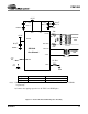
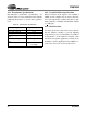
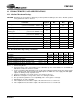
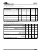
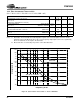
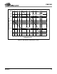

Table Of Contents
- Features
- Description
- 1. Pin Out - 144-Pin LQFP Package
- 2. Pin Out - 160-Ball FBGA Package
- 3. Pin Descriptions
- 4. operation
- 5. Power-up
- 6. Master Clock
- 7. G.772 Monitoring
- 8. Building Integrated Timing Systems (BITS) Clock Mode
- 9. Transmitter
- 10. Receiver
- 11. Jitter Attenuator
- 12. Operational Summary
- 13. Host Mode
- 14. Register Descriptions
- 14.1 Revision/IDcode Register (00h)
- 14.2 Analog Loopback Register (01h)
- 14.3 Remote Loopback Register (02h)
- 14.4 TAOS Enable Register (03h)
- 14.5 LOS Status Register (04h)
- 14.6 DFM Status Register (05h)
- 14.7 LOS Interrupt Enable Register (06h)
- 14.8 DFM Interrupt Enable Register (07h)
- 14.9 LOS Interrupt Status Register (08h)
- 14.10 DFM Interrupt Status Register (09h)
- 14.11 Software Reset Register (0Ah)
- 14.12 Performance Monitor Register (0Bh)
- 14.13 Digital Loopback Reset Register (0Ch)
- 14.14 LOS/AIS Mode Enable Register (0Dh)
- 14.15 Automatic TAOS Register (0Eh)
- 14.16 Global Control Register (0Fh)
- 14.17 Line Length Channel ID Register (10h)
- 14.18 Line Length Data Register (11h)
- 14.19 Output Disable Register (12h)
- 14.20 AIS Status Register (13h)
- 14.21 AIS Interrupt Enable Register (14h)
- 14.22 AIS Interrupt Status Register (15h)
- 14.23 AWG Broadcast Register (16h)
- 14.24 AWG Phase Address Register (17h)
- 14.25 AWG Phase Data Register (18h)
- 14.26 AWG Enable Register (19h)
- 14.27 Reserved Register (1Ah)
- 14.28 Reserved Register (1Bh)
- 14.29 Reserved Register (1Ch)
- 14.30 Reserved Register (1Dh)
- 14.31 Bits Clock Enable Register (1Eh)
- 14.32 Reserved Register (1Fh)
- 14.33 Status Registers
- 15. Arbitrary Waveform Generator
- 16. JTAG Support
- 17. Boundary Scan Register (BSR)
- 18. Applications
- 19. Characteristics and specifications
- 19.1 Absolute Maximum Ratings
- 19.2 Recommended Operating Conditions
- 19.3 Digital Characteristics
- 19.4 Transmitter Analog Characteristics
- 19.5 Receiver Analog Characteristics
- 19.6 Jitter Attenuator Characteristics
- 19.7 Master Clock Switching Characteristics
- 19.8 Transmit Switching Characteristics
- 19.9 Receive Switching Characteristics
- 19.10 Switching Characteristics - Serial Port
- 19.11 Switching Characteristics - Parallel Port (Multiplexed Mode)
- 19.12 Switching Characteristics- Parallel Port (Non-Multiplexed Mode)
- 19.13 Switching Characteristics - JTAG
- 20. Compliant Recommendations and specifications
- 21. 160-Ball FBGA package dimensions
- 22. 144-Pin LQFP Package dimensions
CS61880
58 DS450PP3
19.7 Master Clock Switching Characteristics
19.8 Transmit Switching Characteristics
19.9 Receive Switching Characteristics
Notes: 19. Output load capacitance = 50 pF.
20. MCLK is not active.
Parameter Symbol Min. Typ Max Units
MASTER CLOCK (MCLK)
Master Clock Frequency MCLK 2.048 MHz
Master Clock Tolerance - -100 +100 ppm
Master Clock Duty Cycle - 40 50 60 %
Parameter Symbol Min. Typ Max Units
TCLK Frequency 1/t
pw2
- 2.048 - MHz
TPOS/TNEG Pulse Width (RZ Mode) 236 244 252 ns
TCLK Tolerance (NRZ Mode) -50 - 50 PPM
TCLK Duty Cycle t
pwh2
/t
pw2
--90%
TCLK Pulse Width 20 - - ns
TCLK Burst Rate Note 10 --20MHz
TPOS/TNEG to TCLK Falling Setup Time (NRZ Mode) t
su2
25 - - ns
TCLK Falling to TPOS/TNEG Hold time (NRZ Mode) t
h2
25 - - ns
TXOE Asserted Low to TX Driver HIGH-Z - - 1 µs
TCLK Held Low to Driver HIGH-Z Note 20 81220µs
Parameter Symbol Min. Typ Max Units
RCLK Duty Cycle Note 10 40 50 60 %
RCLK Pulse Width Note 10 196 244 328 ns
RPOS/RNEG Pulse Width (RZ Mode) Note 10 200 244 300 ns
RPOS/RNEG to RCLK rising setup time Note 10 t
su
200 244 ns
RPOS/RNEG to RCLK hold time Note 10 t
h
200 244 ns
RPOS/RNEG Output to RCLK Output (RZ Mode) Note 10 - - 10 ns
Rise/Fall Time, RPOS, RNEG, RCLK, LOS outputs Note 19 t
r
, t
f
- - 85 ns