
User Manual
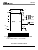
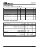
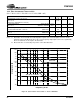
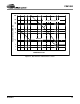

Table Of Contents
- Features
- Description
- 1. Pin Out - 144-Pin LQFP Package
- 2. Pin Out - 160-Ball FBGA Package
- 3. Pin Descriptions
- 4. operation
- 5. Power-up
- 6. Master Clock
- 7. G.772 Monitoring
- 8. Building Integrated Timing Systems (BITS) Clock Mode
- 9. Transmitter
- 10. Receiver
- 11. Jitter Attenuator
- 12. Operational Summary
- 13. Host Mode
- 14. Register Descriptions
- 14.1 Revision/IDcode Register (00h)
- 14.2 Analog Loopback Register (01h)
- 14.3 Remote Loopback Register (02h)
- 14.4 TAOS Enable Register (03h)
- 14.5 LOS Status Register (04h)
- 14.6 DFM Status Register (05h)
- 14.7 LOS Interrupt Enable Register (06h)
- 14.8 DFM Interrupt Enable Register (07h)
- 14.9 LOS Interrupt Status Register (08h)
- 14.10 DFM Interrupt Status Register (09h)
- 14.11 Software Reset Register (0Ah)
- 14.12 Performance Monitor Register (0Bh)
- 14.13 Digital Loopback Reset Register (0Ch)
- 14.14 LOS/AIS Mode Enable Register (0Dh)
- 14.15 Automatic TAOS Register (0Eh)
- 14.16 Global Control Register (0Fh)
- 14.17 Line Length Channel ID Register (10h)
- 14.18 Line Length Data Register (11h)
- 14.19 Output Disable Register (12h)
- 14.20 AIS Status Register (13h)
- 14.21 AIS Interrupt Enable Register (14h)
- 14.22 AIS Interrupt Status Register (15h)
- 14.23 AWG Broadcast Register (16h)
- 14.24 AWG Phase Address Register (17h)
- 14.25 AWG Phase Data Register (18h)
- 14.26 AWG Enable Register (19h)
- 14.27 Reserved Register (1Ah)
- 14.28 Reserved Register (1Bh)
- 14.29 Reserved Register (1Ch)
- 14.30 Reserved Register (1Dh)
- 14.31 Bits Clock Enable Register (1Eh)
- 14.32 Reserved Register (1Fh)
- 14.33 Status Registers
- 15. Arbitrary Waveform Generator
- 16. JTAG Support
- 17. Boundary Scan Register (BSR)
- 18. Applications
- 19. Characteristics and specifications
- 19.1 Absolute Maximum Ratings
- 19.2 Recommended Operating Conditions
- 19.3 Digital Characteristics
- 19.4 Transmitter Analog Characteristics
- 19.5 Receiver Analog Characteristics
- 19.6 Jitter Attenuator Characteristics
- 19.7 Master Clock Switching Characteristics
- 19.8 Transmit Switching Characteristics
- 19.9 Receive Switching Characteristics
- 19.10 Switching Characteristics - Serial Port
- 19.11 Switching Characteristics - Parallel Port (Multiplexed Mode)
- 19.12 Switching Characteristics- Parallel Port (Non-Multiplexed Mode)
- 19.13 Switching Characteristics - JTAG
- 20. Compliant Recommendations and specifications
- 21. 160-Ball FBGA package dimensions
- 22. 144-Pin LQFP Package dimensions
CS61880
56 DS450PP3
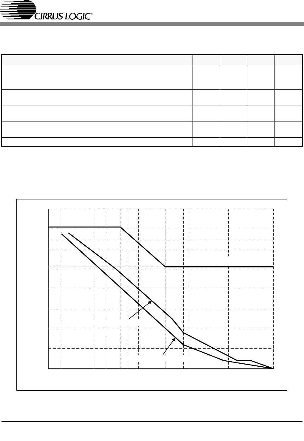
19.6 Jitter Attenuator Characteristics
(TA = -40° C to 85° C; TV+, RV+ = 3.3 V ±5%; GND = 0 V)
Notes: 17. Attenuation measured with sinusoidal input filter equal to 3/4 of measured jitter tolerance. Circuit
attenuates jitter at 20 dB/decade above the corner frequency. Output jitter can increase significantly
when more than 28 UI’s are input to the attenuator.
18. Measurement is not effected by the position of the Jitter Attenuator.
Parameter Min. Typ Max Units
Jitter Attenuator Corner Frequency
Note 10, 18
(Depends on JACF Bit in host mode)
-
-
1.25
2.50
-
-
Hz
E1 Jitter Attenuation 3 Hz to 40 Hz
Note 10, 17 400 Hz to 100 kHz
+ 0.5
-19.5
-
-
-
-
dB
Attenuator Input Jitter Tolerance before FIFO 32-bit FIFO
over flow and under flow Note 10 64-bit FIFO
-
-
24
56
-
-
UI
UI
Delay through Jitter Attenuator Only 32-bit FIFO
Note 10 64-bit FIFO
-
-
16
32
-
-
UI
UI
Intrinsic Jitter in Remote Loopback Notes 10, 16 --0.11UI
110
100
1K 10K
0
Attenuation in dB
Frequency in Hz
+ 0.5
2
57
1.4K20 40040
+ 10
- 10
- 20
- 30
- 50
- 40
- 60
- 19.5
- 6
- 70
100K
ITU G.736
TYP. E1 @ 1.25 Hz CF
TYP. E1 @ 2.5 Hz CF
Figure 18. Jitter Transfer Characteristic vs. G.736 & TBR 12/13