
User Manual
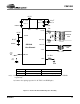
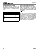
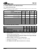
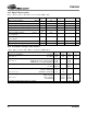
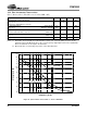

Table Of Contents
- Features
- Description
- 1. Pin Out - 144-Pin LQFP Package
- 2. Pin Out - 160-Ball FBGA Package
- 3. Pin Descriptions
- 4. operation
- 5. Power-up
- 6. Master Clock
- 7. G.772 Monitoring
- 8. Building Integrated Timing Systems (BITS) Clock Mode
- 9. Transmitter
- 10. Receiver
- 11. Jitter Attenuator
- 12. Operational Summary
- 13. Host Mode
- 14. Register Descriptions
- 14.1 Revision/IDcode Register (00h)
- 14.2 Analog Loopback Register (01h)
- 14.3 Remote Loopback Register (02h)
- 14.4 TAOS Enable Register (03h)
- 14.5 LOS Status Register (04h)
- 14.6 DFM Status Register (05h)
- 14.7 LOS Interrupt Enable Register (06h)
- 14.8 DFM Interrupt Enable Register (07h)
- 14.9 LOS Interrupt Status Register (08h)
- 14.10 DFM Interrupt Status Register (09h)
- 14.11 Software Reset Register (0Ah)
- 14.12 Performance Monitor Register (0Bh)
- 14.13 Digital Loopback Reset Register (0Ch)
- 14.14 LOS/AIS Mode Enable Register (0Dh)
- 14.15 Automatic TAOS Register (0Eh)
- 14.16 Global Control Register (0Fh)
- 14.17 Line Length Channel ID Register (10h)
- 14.18 Line Length Data Register (11h)
- 14.19 Output Disable Register (12h)
- 14.20 AIS Status Register (13h)
- 14.21 AIS Interrupt Enable Register (14h)
- 14.22 AIS Interrupt Status Register (15h)
- 14.23 AWG Broadcast Register (16h)
- 14.24 AWG Phase Address Register (17h)
- 14.25 AWG Phase Data Register (18h)
- 14.26 AWG Enable Register (19h)
- 14.27 Reserved Register (1Ah)
- 14.28 Reserved Register (1Bh)
- 14.29 Reserved Register (1Ch)
- 14.30 Reserved Register (1Dh)
- 14.31 Bits Clock Enable Register (1Eh)
- 14.32 Reserved Register (1Fh)
- 14.33 Status Registers
- 15. Arbitrary Waveform Generator
- 16. JTAG Support
- 17. Boundary Scan Register (BSR)
- 18. Applications
- 19. Characteristics and specifications
- 19.1 Absolute Maximum Ratings
- 19.2 Recommended Operating Conditions
- 19.3 Digital Characteristics
- 19.4 Transmitter Analog Characteristics
- 19.5 Receiver Analog Characteristics
- 19.6 Jitter Attenuator Characteristics
- 19.7 Master Clock Switching Characteristics
- 19.8 Transmit Switching Characteristics
- 19.9 Receive Switching Characteristics
- 19.10 Switching Characteristics - Serial Port
- 19.11 Switching Characteristics - Parallel Port (Multiplexed Mode)
- 19.12 Switching Characteristics- Parallel Port (Non-Multiplexed Mode)
- 19.13 Switching Characteristics - JTAG
- 20. Compliant Recommendations and specifications
- 21. 160-Ball FBGA package dimensions
- 22. 144-Pin LQFP Package dimensions
CS61880
DS450PP3 55
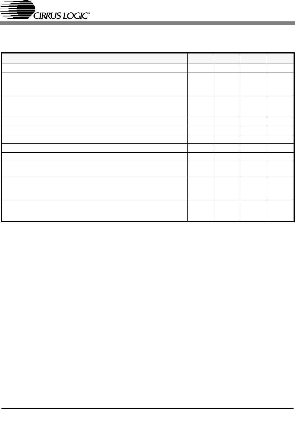
19.5 Receiver Analog Characteristics
(TA = -40° C to 85° C; TV+, RV+ = 3.3 V ±5%; GND = 0 V))
Notes: 10. Parameters guaranteed by design and characterization.
11. Using components on the CDB61880 evaluation board in Internal Match Impedance Mode.
12. Return loss = 20log10 ABS((Z1 + Z0) / (Z1 - Z0)) where Z1 - impedance of the transmitter or receiver,
and Z0 = cable impedance.
13. Assuming that jitter free clock is input to TCLK.
14. Jitter tolerance for 6 dB input signal levels. Jitter tolerance increases at lower frequencies. HDB3 coders
enabled.
15. In Data Recovery Mode.
16. Jitter Attenuator in the receive path.
Parameter Min. Typ Max Units
Allowable Cable Attenuation @ 1024 kHz - - - 12 dB
RTIP/RRING Input Impedance E1 120 Ω Load
(Internal Line matching mode) E1 75 Ω Load
Note 10
-
-
13k
50
-
-
Ω
RTIP/RRING Input Impedance E1 120 Ω Load
(External Line matching mode) E1 75 Ω Load
Note 10
-
-
13k
13k
-
-
Ω
Receiver Dynamic Range 0.5 - - Vp
Signal to Noise margin (Per G.703, O151 @ 6 dB cable Atten). - -18 - dB
Receiver Squelch Level 150 mV
LOS Threshold - 200 - mV
LOS Hysteresis 50 mV
Data Decision Threshold
Note 10
41 50 59 % of
peak
Input Jitter Tolerance 1 Hz - 1.8 Hz
Notes 10, 14, 16 20 Hz - 2.4 kHz
18 kHz - 100 kHz
18
1.5
0.2
-
-
-
-
-
-
UI
Input Return Loss 51 kHz - 102 kHz
102 kHz - 2048 kHz
Notes 10, 11, 12 2048 kHz - 3072 kHz
-18
-18
-18
-28
-30
-27
-
-
-
dB