
User Manual
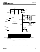
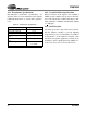
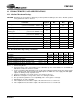
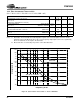
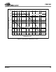

Table Of Contents
- Features
- Description
- 1. Pin Out - 144-Pin LQFP Package
- 2. Pin Out - 160-Ball FBGA Package
- 3. Pin Descriptions
- 4. operation
- 5. Power-up
- 6. Master Clock
- 7. G.772 Monitoring
- 8. Building Integrated Timing Systems (BITS) Clock Mode
- 9. Transmitter
- 10. Receiver
- 11. Jitter Attenuator
- 12. Operational Summary
- 13. Host Mode
- 14. Register Descriptions
- 14.1 Revision/IDcode Register (00h)
- 14.2 Analog Loopback Register (01h)
- 14.3 Remote Loopback Register (02h)
- 14.4 TAOS Enable Register (03h)
- 14.5 LOS Status Register (04h)
- 14.6 DFM Status Register (05h)
- 14.7 LOS Interrupt Enable Register (06h)
- 14.8 DFM Interrupt Enable Register (07h)
- 14.9 LOS Interrupt Status Register (08h)
- 14.10 DFM Interrupt Status Register (09h)
- 14.11 Software Reset Register (0Ah)
- 14.12 Performance Monitor Register (0Bh)
- 14.13 Digital Loopback Reset Register (0Ch)
- 14.14 LOS/AIS Mode Enable Register (0Dh)
- 14.15 Automatic TAOS Register (0Eh)
- 14.16 Global Control Register (0Fh)
- 14.17 Line Length Channel ID Register (10h)
- 14.18 Line Length Data Register (11h)
- 14.19 Output Disable Register (12h)
- 14.20 AIS Status Register (13h)
- 14.21 AIS Interrupt Enable Register (14h)
- 14.22 AIS Interrupt Status Register (15h)
- 14.23 AWG Broadcast Register (16h)
- 14.24 AWG Phase Address Register (17h)
- 14.25 AWG Phase Data Register (18h)
- 14.26 AWG Enable Register (19h)
- 14.27 Reserved Register (1Ah)
- 14.28 Reserved Register (1Bh)
- 14.29 Reserved Register (1Ch)
- 14.30 Reserved Register (1Dh)
- 14.31 Bits Clock Enable Register (1Eh)
- 14.32 Reserved Register (1Fh)
- 14.33 Status Registers
- 15. Arbitrary Waveform Generator
- 16. JTAG Support
- 17. Boundary Scan Register (BSR)
- 18. Applications
- 19. Characteristics and specifications
- 19.1 Absolute Maximum Ratings
- 19.2 Recommended Operating Conditions
- 19.3 Digital Characteristics
- 19.4 Transmitter Analog Characteristics
- 19.5 Receiver Analog Characteristics
- 19.6 Jitter Attenuator Characteristics
- 19.7 Master Clock Switching Characteristics
- 19.8 Transmit Switching Characteristics
- 19.9 Receive Switching Characteristics
- 19.10 Switching Characteristics - Serial Port
- 19.11 Switching Characteristics - Parallel Port (Multiplexed Mode)
- 19.12 Switching Characteristics- Parallel Port (Non-Multiplexed Mode)
- 19.13 Switching Characteristics - JTAG
- 20. Compliant Recommendations and specifications
- 21. 160-Ball FBGA package dimensions
- 22. 144-Pin LQFP Package dimensions
CS61880
DS450PP3 53
19. CHARACTERISTICS AND SPECIFICATIONS
19.1 Absolute Maximum Ratings
CAUTION: Operations at or beyond these limits may result in permanent damage to the device. Normal operation
is not guaranteed at these extremes.
19.2 Recommended Operating Conditions
Notes: 1. Human Body Model
2. Transient current of up to 100 mA will not cause SCR latch-up. Also TTIP, TRING, TV+ and TGND can
withstand a continuous current of 100 mA.
3. Power consumption while driving line load over the full operating temperature and power supply voltage
range. Includes all IC channels and loads. Digital inputs are within 10% of the supply rails and digital
outputs are driving a 50 pF capacitive load.
4. Typical consumption corresponds to 50% ones density for at 3.3 V.
5. Maximum consumption corresponds to 100% ones density at 3.465 V.
6. This specification guarantees TTL compatibility (V
OH
= 2.4 V @ I
OUT
= -400 µA).
7. Output drivers are TTL compatible.
8. Pulse amplitude measured at the output of the transformer across a 75 Ω load.
9. Pulse amplitude measured at the output of the transformer across a 120 Ω load.
Parameter Symbol Min. Max Units
DC Supply
(referenced to RGND = TGND = 0V)
RV+
TV+
-
-
4.0
4.0
V
V
DC Supply VCCIO -0.5 4.6 V
Input Voltage, Any Digital Pin except CBLSEL, MODE and
LOOP(n) pins (referenced to GNDIO = 0V)
V
IH
GNDIO -0.5 5.3 V
Input Voltage CBLSEL, MODE & LOOP(n) Pins
(referenced to GNDIO = 0V)
V
IH
GNDIO -0.5 VCCIO +0.5 V
Input voltage, RTIP and RRING Pins TGND -0.5 TV+ +0.5 V
ESD voltage, Any pin Note 1 2k - V
Input current, Any Pin Note 2 I
IH
-10 +10 mA
Maximum Power Dissipation, In package P
p
-1.73W
Ambient Operating Temperature T
A
-40 85 C
Storage Temperature T
stg
-65 150 C
Parameter Symbol Min. Typ Max Units
DC Supply RV+, TV+ 3.135 3.3 3.465 V
DC Supply VCCIO 3.135 3.3 3.465 V
Ambient operating Temperature T
A
-40 25 85 C
Power Consumption, E1 Mode, 75 Ω line load Notes 3, 4, 5
-
- 660 1040 mW
Power Consumption, E1 Mode, 120 Ω line load Notes 3, 4, 5
-
- 640 950 mW