
User Manual
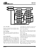
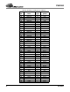
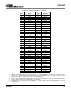
Table Of Contents
- Features
- Description
- 1. Pin Out - 144-Pin LQFP Package
- 2. Pin Out - 160-Ball FBGA Package
- 3. Pin Descriptions
- 4. operation
- 5. Power-up
- 6. Master Clock
- 7. G.772 Monitoring
- 8. Building Integrated Timing Systems (BITS) Clock Mode
- 9. Transmitter
- 10. Receiver
- 11. Jitter Attenuator
- 12. Operational Summary
- 13. Host Mode
- 14. Register Descriptions
- 14.1 Revision/IDcode Register (00h)
- 14.2 Analog Loopback Register (01h)
- 14.3 Remote Loopback Register (02h)
- 14.4 TAOS Enable Register (03h)
- 14.5 LOS Status Register (04h)
- 14.6 DFM Status Register (05h)
- 14.7 LOS Interrupt Enable Register (06h)
- 14.8 DFM Interrupt Enable Register (07h)
- 14.9 LOS Interrupt Status Register (08h)
- 14.10 DFM Interrupt Status Register (09h)
- 14.11 Software Reset Register (0Ah)
- 14.12 Performance Monitor Register (0Bh)
- 14.13 Digital Loopback Reset Register (0Ch)
- 14.14 LOS/AIS Mode Enable Register (0Dh)
- 14.15 Automatic TAOS Register (0Eh)
- 14.16 Global Control Register (0Fh)
- 14.17 Line Length Channel ID Register (10h)
- 14.18 Line Length Data Register (11h)
- 14.19 Output Disable Register (12h)
- 14.20 AIS Status Register (13h)
- 14.21 AIS Interrupt Enable Register (14h)
- 14.22 AIS Interrupt Status Register (15h)
- 14.23 AWG Broadcast Register (16h)
- 14.24 AWG Phase Address Register (17h)
- 14.25 AWG Phase Data Register (18h)
- 14.26 AWG Enable Register (19h)
- 14.27 Reserved Register (1Ah)
- 14.28 Reserved Register (1Bh)
- 14.29 Reserved Register (1Ch)
- 14.30 Reserved Register (1Dh)
- 14.31 Bits Clock Enable Register (1Eh)
- 14.32 Reserved Register (1Fh)
- 14.33 Status Registers
- 15. Arbitrary Waveform Generator
- 16. JTAG Support
- 17. Boundary Scan Register (BSR)
- 18. Applications
- 19. Characteristics and specifications
- 19.1 Absolute Maximum Ratings
- 19.2 Recommended Operating Conditions
- 19.3 Digital Characteristics
- 19.4 Transmitter Analog Characteristics
- 19.5 Receiver Analog Characteristics
- 19.6 Jitter Attenuator Characteristics
- 19.7 Master Clock Switching Characteristics
- 19.8 Transmit Switching Characteristics
- 19.9 Receive Switching Characteristics
- 19.10 Switching Characteristics - Serial Port
- 19.11 Switching Characteristics - Parallel Port (Multiplexed Mode)
- 19.12 Switching Characteristics- Parallel Port (Non-Multiplexed Mode)
- 19.13 Switching Characteristics - JTAG
- 20. Compliant Recommendations and specifications
- 21. 160-Ball FBGA package dimensions
- 22. 144-Pin LQFP Package dimensions
CS61880
DS450PP3 49
Notes:
1) LPOEN controls the LOOP[7:0] pins. Setting LPOEN to “1” configures LOOP[7:0] as outputs. The output value driven
on the pins are determined by the values written to LPO[7:0]. Setting LPOEN to “0” High-Z all the pins. In this mode,
the input values driven to these LOOP[7:0] can be read via LPI[7:0].
2) HIZ_B controls the RPOSx, RNEGx, and RCLKx pins. When HIZ_B is High, the outputs are enabled; when HIZ_B is
Low, the outputs are placed in a high impedance state (High-Z).
3) RDYOEN controls the ACK_B pin. Setting RDYOEN to “1” enables output on ACK_B. Setting ACKEN to “0” High -Z
the ACK_B pin.
73 TCLK3 I TCLK3
74 LOS2 O LOS2
75 RNEG2 O RNEG2
76 RPOS2 O RPOS2
77 RCLK2 O RCLK2
78 - Note 2 HIZ2_B
79 TNEG2 I TNEG2
80 TPOS2 I TPOS2
81 TCLK2 I TCLK2
82 INT_B O INT_B
83 RDY O RDYOUT
84 - Note 3 RDYOEN
85 WR_B I WR_B
86 RD_B I RD_B
87 ALE I ALE
88 CS_B I CS_B
89 CS_B I CS_B_TRI
90 INTL I INTL
91 CBLSEL I CBLSEL_TRI
92 CBLSEL I CBLSEL_IN
93 TCLK5 I TCLK5
94 TPOS5 I TPOS5
95 TNEG5 I TNEG5
96 RCLK5 O RCLK5
97 RPOS5 O RPOS5
98 RNEG5 O RNEG5
99 - Note 2 HIZ5_B
100 LOS5 O LOS5
101 TCLK4 I TCLK4
102 TPOS4 I TPOS4
103 TNEG4 I TNEG4
104 RCLK4 O RCLK4
105 RPOS4 O RPOS4
106 RNEG4 O RNEG4
107 - Note 2 HIZ4_B
108 LOS4 O LOS4
109 TXOE I TXOE
110 CLKE I CLKE
Table 14. Boundary Scan Register (Continued)
BSR
Bit
Pin
Name
Cell
Type
Bit
Symbol