
User Manual
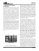
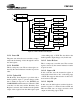
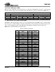
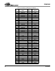
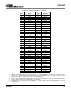
Table Of Contents
- Features
- Description
- 1. Pin Out - 144-Pin LQFP Package
- 2. Pin Out - 160-Ball FBGA Package
- 3. Pin Descriptions
- 4. operation
- 5. Power-up
- 6. Master Clock
- 7. G.772 Monitoring
- 8. Building Integrated Timing Systems (BITS) Clock Mode
- 9. Transmitter
- 10. Receiver
- 11. Jitter Attenuator
- 12. Operational Summary
- 13. Host Mode
- 14. Register Descriptions
- 14.1 Revision/IDcode Register (00h)
- 14.2 Analog Loopback Register (01h)
- 14.3 Remote Loopback Register (02h)
- 14.4 TAOS Enable Register (03h)
- 14.5 LOS Status Register (04h)
- 14.6 DFM Status Register (05h)
- 14.7 LOS Interrupt Enable Register (06h)
- 14.8 DFM Interrupt Enable Register (07h)
- 14.9 LOS Interrupt Status Register (08h)
- 14.10 DFM Interrupt Status Register (09h)
- 14.11 Software Reset Register (0Ah)
- 14.12 Performance Monitor Register (0Bh)
- 14.13 Digital Loopback Reset Register (0Ch)
- 14.14 LOS/AIS Mode Enable Register (0Dh)
- 14.15 Automatic TAOS Register (0Eh)
- 14.16 Global Control Register (0Fh)
- 14.17 Line Length Channel ID Register (10h)
- 14.18 Line Length Data Register (11h)
- 14.19 Output Disable Register (12h)
- 14.20 AIS Status Register (13h)
- 14.21 AIS Interrupt Enable Register (14h)
- 14.22 AIS Interrupt Status Register (15h)
- 14.23 AWG Broadcast Register (16h)
- 14.24 AWG Phase Address Register (17h)
- 14.25 AWG Phase Data Register (18h)
- 14.26 AWG Enable Register (19h)
- 14.27 Reserved Register (1Ah)
- 14.28 Reserved Register (1Bh)
- 14.29 Reserved Register (1Ch)
- 14.30 Reserved Register (1Dh)
- 14.31 Bits Clock Enable Register (1Eh)
- 14.32 Reserved Register (1Fh)
- 14.33 Status Registers
- 15. Arbitrary Waveform Generator
- 16. JTAG Support
- 17. Boundary Scan Register (BSR)
- 18. Applications
- 19. Characteristics and specifications
- 19.1 Absolute Maximum Ratings
- 19.2 Recommended Operating Conditions
- 19.3 Digital Characteristics
- 19.4 Transmitter Analog Characteristics
- 19.5 Receiver Analog Characteristics
- 19.6 Jitter Attenuator Characteristics
- 19.7 Master Clock Switching Characteristics
- 19.8 Transmit Switching Characteristics
- 19.9 Receive Switching Characteristics
- 19.10 Switching Characteristics - Serial Port
- 19.11 Switching Characteristics - Parallel Port (Multiplexed Mode)
- 19.12 Switching Characteristics- Parallel Port (Non-Multiplexed Mode)
- 19.13 Switching Characteristics - JTAG
- 20. Compliant Recommendations and specifications
- 21. 160-Ball FBGA package dimensions
- 22. 144-Pin LQFP Package dimensions
CS61880
DS450PP3 47
16.3 Device ID Register (IDR)
Revision section: 0h = Rev A, 1h = Rev B and so on. The device Identification Code [27 - 12] is derived
from the last three digits of the part number (880). The LSB is a constant 1, as defined by IEEE 1149.1.
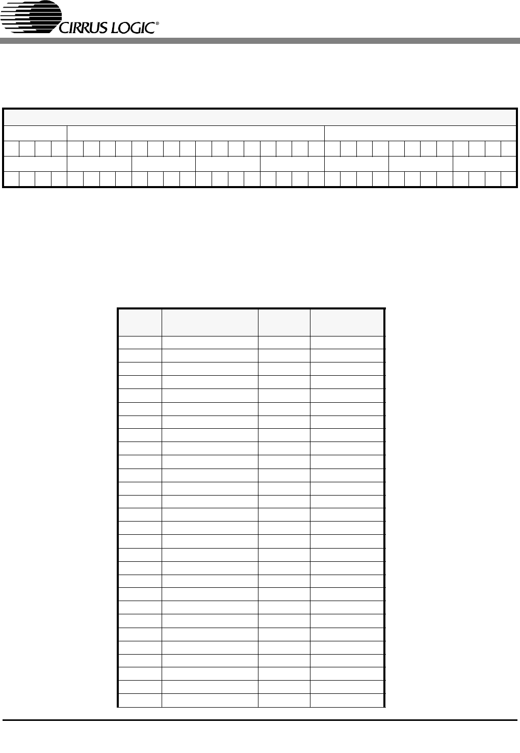
17. BOUNDARY SCAN REGISTER (BSR)
The BSR is a shift register that provides access to the digital I/O pins. The BSR is used to read and write
the device pins to verify interchip connectivity. Each pin has a corresponding scan cell in the register. The
pin to scan cell mapping is given in the Boundary Scan Register description shown in Table 14.
NOTE: Data is shifted LSB first into the BSR register.
CS61880 IDCODE REGISTER(IDR)
REVISION DEVICE IDCODE REGISTER MANUFACTURER CODE
31 30 29 28 27 26 25 24 23 22 21 20 19 18 17 16 15 14 13 12 11 10 9 8 7 6 5 4 3 2 1 0
0h 0h 8h 8h 0h 0h Ch 9h
00000000100010000000000011001001
Table 14. Boundary Scan Register
BSR
Bit
Pin
Name
Cell
Type
Bit
Symbol
0 LOS7 O LOS7
1 RNEG7 O RNEG7
2 RPOS7 O RPOS7
3 RCLK7 O RCLK7
4 - Note 2 HIZ7_B
5 TNEG7 I TNEG7
6 TPOS7 I TPOS7
7 TCLK7 I TCLK7
8 LOS6 O LOS6_B
9 RNEG6 O RNEG6
10 RPOS6 O RPOS6
11 RCLK6 O RCLK6
12 - Note 2 HIZ6_B
13 TNEG6 I TNEG6
14 TPOS6 I TPOS6
15 TCLK6 I TCLK6
16 MCLK I MCLK
17 MODE I MODE_TRI
18 MODE I MODE_IN
19 ADDR4 I ADDR4
20 ADDR3 I ADDR3
21 ADDR2 I ADDR2
22 ADDR1 I ADDR1
23 ADDR0 I ADDR0
24 LOOP0/D0 I LPT0
25 LOOP0/D0 I LPI0
26 LOOP0/D0 O LPO0
27 LOOP1/D1 I LPT1