
User Manual
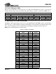
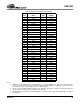
Table Of Contents
- Features
- Description
- 1. Pin Out - 144-Pin LQFP Package
- 2. Pin Out - 160-Ball FBGA Package
- 3. Pin Descriptions
- 4. operation
- 5. Power-up
- 6. Master Clock
- 7. G.772 Monitoring
- 8. Building Integrated Timing Systems (BITS) Clock Mode
- 9. Transmitter
- 10. Receiver
- 11. Jitter Attenuator
- 12. Operational Summary
- 13. Host Mode
- 14. Register Descriptions
- 14.1 Revision/IDcode Register (00h)
- 14.2 Analog Loopback Register (01h)
- 14.3 Remote Loopback Register (02h)
- 14.4 TAOS Enable Register (03h)
- 14.5 LOS Status Register (04h)
- 14.6 DFM Status Register (05h)
- 14.7 LOS Interrupt Enable Register (06h)
- 14.8 DFM Interrupt Enable Register (07h)
- 14.9 LOS Interrupt Status Register (08h)
- 14.10 DFM Interrupt Status Register (09h)
- 14.11 Software Reset Register (0Ah)
- 14.12 Performance Monitor Register (0Bh)
- 14.13 Digital Loopback Reset Register (0Ch)
- 14.14 LOS/AIS Mode Enable Register (0Dh)
- 14.15 Automatic TAOS Register (0Eh)
- 14.16 Global Control Register (0Fh)
- 14.17 Line Length Channel ID Register (10h)
- 14.18 Line Length Data Register (11h)
- 14.19 Output Disable Register (12h)
- 14.20 AIS Status Register (13h)
- 14.21 AIS Interrupt Enable Register (14h)
- 14.22 AIS Interrupt Status Register (15h)
- 14.23 AWG Broadcast Register (16h)
- 14.24 AWG Phase Address Register (17h)
- 14.25 AWG Phase Data Register (18h)
- 14.26 AWG Enable Register (19h)
- 14.27 Reserved Register (1Ah)
- 14.28 Reserved Register (1Bh)
- 14.29 Reserved Register (1Ch)
- 14.30 Reserved Register (1Dh)
- 14.31 Bits Clock Enable Register (1Eh)
- 14.32 Reserved Register (1Fh)
- 14.33 Status Registers
- 15. Arbitrary Waveform Generator
- 16. JTAG Support
- 17. Boundary Scan Register (BSR)
- 18. Applications
- 19. Characteristics and specifications
- 19.1 Absolute Maximum Ratings
- 19.2 Recommended Operating Conditions
- 19.3 Digital Characteristics
- 19.4 Transmitter Analog Characteristics
- 19.5 Receiver Analog Characteristics
- 19.6 Jitter Attenuator Characteristics
- 19.7 Master Clock Switching Characteristics
- 19.8 Transmit Switching Characteristics
- 19.9 Receive Switching Characteristics
- 19.10 Switching Characteristics - Serial Port
- 19.11 Switching Characteristics - Parallel Port (Multiplexed Mode)
- 19.12 Switching Characteristics- Parallel Port (Non-Multiplexed Mode)
- 19.13 Switching Characteristics - JTAG
- 20. Compliant Recommendations and specifications
- 21. 160-Ball FBGA package dimensions
- 22. 144-Pin LQFP Package dimensions
CS61880
46 DS450PP3
16.1.14 Exit1-IR
This is a temporary state. The test data register se-
lected by the current instruction retains its previous
value.
16.1.15 Pause-IR
The pause state allows the test controller to tempo-
rarily halt the shifting of data through the instruc-
tion register.
16.1.16 Exit2-IR
This is a temporary state. The test data register se-
lected by the current instruction retains its previous
value.
16.1.17 Update-IR
The instruction shifted into the instruction register
is latched into the parallel output from the shift-reg-
ister path on the falling edge of TCK. When the
new instruction has been latched, it becomes the
current instruction. The test data registers selected
by the current instruction retain their previous val-
ue.
16.2 Instruction Register (IR)
The 3-bit Instruction register selects the test to be
performed and/or the data register to be accessed.
The valid instructions are shifted in LSB first and
are listed in Table 13:
16.2.1 EXTEST
The EXTEST instruction allows testing of off-chip
circuitry and board-level interconnect. EXTEST
connects the BSR to the TDI and TDO pins.
16.2.2 SAMPLE/PRELOAD
The SAMPLE/PRELOAD instruction samples all
device inputs and outputs. This instruction places
the BSR between the TDI and TDO pins. The BSR
is loaded with samples of the I/O pins by the Cap-
ture-DR state.
16.2.3 IDCODE
The IDCODE instruction connects the device iden-
tification register to the TDO pin. The device iden-
tification code can then be shifted out TDO using
the Shift-DR state.
16.2.4 BYPASS
The BYPASS instruction connects a one TCK de-
lay register between TDI and TDO. The instruction
is used to bypass the device.
Table 13. JTAG Instructions
IR CODE INSTRUCTION
000 EXTEST
100 SAMPLE/PRELOAD
110 IDCODE
111 BYPASS