
User Manual
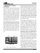
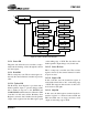
Table Of Contents
- Features
- Description
- 1. Pin Out - 144-Pin LQFP Package
- 2. Pin Out - 160-Ball FBGA Package
- 3. Pin Descriptions
- 4. operation
- 5. Power-up
- 6. Master Clock
- 7. G.772 Monitoring
- 8. Building Integrated Timing Systems (BITS) Clock Mode
- 9. Transmitter
- 10. Receiver
- 11. Jitter Attenuator
- 12. Operational Summary
- 13. Host Mode
- 14. Register Descriptions
- 14.1 Revision/IDcode Register (00h)
- 14.2 Analog Loopback Register (01h)
- 14.3 Remote Loopback Register (02h)
- 14.4 TAOS Enable Register (03h)
- 14.5 LOS Status Register (04h)
- 14.6 DFM Status Register (05h)
- 14.7 LOS Interrupt Enable Register (06h)
- 14.8 DFM Interrupt Enable Register (07h)
- 14.9 LOS Interrupt Status Register (08h)
- 14.10 DFM Interrupt Status Register (09h)
- 14.11 Software Reset Register (0Ah)
- 14.12 Performance Monitor Register (0Bh)
- 14.13 Digital Loopback Reset Register (0Ch)
- 14.14 LOS/AIS Mode Enable Register (0Dh)
- 14.15 Automatic TAOS Register (0Eh)
- 14.16 Global Control Register (0Fh)
- 14.17 Line Length Channel ID Register (10h)
- 14.18 Line Length Data Register (11h)
- 14.19 Output Disable Register (12h)
- 14.20 AIS Status Register (13h)
- 14.21 AIS Interrupt Enable Register (14h)
- 14.22 AIS Interrupt Status Register (15h)
- 14.23 AWG Broadcast Register (16h)
- 14.24 AWG Phase Address Register (17h)
- 14.25 AWG Phase Data Register (18h)
- 14.26 AWG Enable Register (19h)
- 14.27 Reserved Register (1Ah)
- 14.28 Reserved Register (1Bh)
- 14.29 Reserved Register (1Ch)
- 14.30 Reserved Register (1Dh)
- 14.31 Bits Clock Enable Register (1Eh)
- 14.32 Reserved Register (1Fh)
- 14.33 Status Registers
- 15. Arbitrary Waveform Generator
- 16. JTAG Support
- 17. Boundary Scan Register (BSR)
- 18. Applications
- 19. Characteristics and specifications
- 19.1 Absolute Maximum Ratings
- 19.2 Recommended Operating Conditions
- 19.3 Digital Characteristics
- 19.4 Transmitter Analog Characteristics
- 19.5 Receiver Analog Characteristics
- 19.6 Jitter Attenuator Characteristics
- 19.7 Master Clock Switching Characteristics
- 19.8 Transmit Switching Characteristics
- 19.9 Receive Switching Characteristics
- 19.10 Switching Characteristics - Serial Port
- 19.11 Switching Characteristics - Parallel Port (Multiplexed Mode)
- 19.12 Switching Characteristics- Parallel Port (Non-Multiplexed Mode)
- 19.13 Switching Characteristics - JTAG
- 20. Compliant Recommendations and specifications
- 21. 160-Ball FBGA package dimensions
- 22. 144-Pin LQFP Package dimensions
CS61880
DS450PP3 45
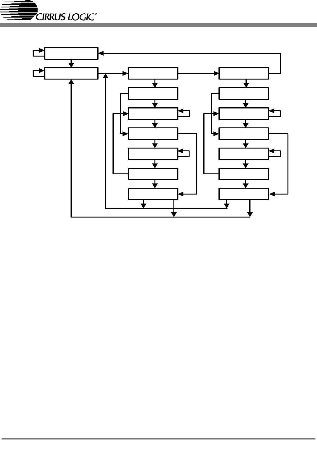
16.1.8 Pause-DR
The pause state allows the test controller to tempo-
rarily halt the shifting of data through the current
test data register.
16.1.9 Exit2-DR
This is a temporary state. The test data register se-
lected by the current instruction retains its previous
value.
16.1.10 Update-DR
The Boundary Scan Register is provided with a
latched parallel output to prevent changes while
data is shifted in response to the EXTEST and
SAMPLE/PRELOAD instructions. When the TAP
controller is in this state and the Boundary Scan
Register is selected, data is latched into the parallel
output of this register from the shift-register path
on the falling edge of TCK. The data held at the
latched parallel output changes only in this state.
16.1.11 Select-IR-Scan
This is a temporary controller state. The test data
register selected by the current instruction retains
its previous state.
16.1.12 Capture-IR
In this controller state, the instruction register is
loaded with a fixed value of “01” on the rising edge
of TCK. This supports fault-isolation of the board-
level serial test data path.
16.1.13 Shift-IR
In this state, the shift register contained in the in-
struction register is connected between TDI and
TDO and shifts data one stage towards its serial
output on each rising edge of TCK.
1
0
Test-Logic-Reset
Run-Test/Idle
Select-DR-Scan
Capture-DR
Shift-DR
Exit1-DR
Pause-DR
Exit2-DR
Update-DR
Select- I R-Scan
Capture- IR
Shift- IR
Exit1- IR
Pause-IR
Exit2- IR
Update- IR
0
11
1
1
1
11
1
1
1
11
1
1
0
0
0
0
0
0
0
0
00
0
0
0
1
0
Figure 15. TAP Controller State Diagram