
User Manual
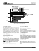
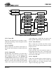
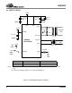
Table Of Contents
- Features
- Description
- 1. Pin Out - 144-Pin LQFP Package
- 2. Pin Out - 160-Ball FBGA Package
- 3. Pin Descriptions
- 4. operation
- 5. Power-up
- 6. Master Clock
- 7. G.772 Monitoring
- 8. Building Integrated Timing Systems (BITS) Clock Mode
- 9. Transmitter
- 10. Receiver
- 11. Jitter Attenuator
- 12. Operational Summary
- 13. Host Mode
- 14. Register Descriptions
- 14.1 Revision/IDcode Register (00h)
- 14.2 Analog Loopback Register (01h)
- 14.3 Remote Loopback Register (02h)
- 14.4 TAOS Enable Register (03h)
- 14.5 LOS Status Register (04h)
- 14.6 DFM Status Register (05h)
- 14.7 LOS Interrupt Enable Register (06h)
- 14.8 DFM Interrupt Enable Register (07h)
- 14.9 LOS Interrupt Status Register (08h)
- 14.10 DFM Interrupt Status Register (09h)
- 14.11 Software Reset Register (0Ah)
- 14.12 Performance Monitor Register (0Bh)
- 14.13 Digital Loopback Reset Register (0Ch)
- 14.14 LOS/AIS Mode Enable Register (0Dh)
- 14.15 Automatic TAOS Register (0Eh)
- 14.16 Global Control Register (0Fh)
- 14.17 Line Length Channel ID Register (10h)
- 14.18 Line Length Data Register (11h)
- 14.19 Output Disable Register (12h)
- 14.20 AIS Status Register (13h)
- 14.21 AIS Interrupt Enable Register (14h)
- 14.22 AIS Interrupt Status Register (15h)
- 14.23 AWG Broadcast Register (16h)
- 14.24 AWG Phase Address Register (17h)
- 14.25 AWG Phase Data Register (18h)
- 14.26 AWG Enable Register (19h)
- 14.27 Reserved Register (1Ah)
- 14.28 Reserved Register (1Bh)
- 14.29 Reserved Register (1Ch)
- 14.30 Reserved Register (1Dh)
- 14.31 Bits Clock Enable Register (1Eh)
- 14.32 Reserved Register (1Fh)
- 14.33 Status Registers
- 15. Arbitrary Waveform Generator
- 16. JTAG Support
- 17. Boundary Scan Register (BSR)
- 18. Applications
- 19. Characteristics and specifications
- 19.1 Absolute Maximum Ratings
- 19.2 Recommended Operating Conditions
- 19.3 Digital Characteristics
- 19.4 Transmitter Analog Characteristics
- 19.5 Receiver Analog Characteristics
- 19.6 Jitter Attenuator Characteristics
- 19.7 Master Clock Switching Characteristics
- 19.8 Transmit Switching Characteristics
- 19.9 Receive Switching Characteristics
- 19.10 Switching Characteristics - Serial Port
- 19.11 Switching Characteristics - Parallel Port (Multiplexed Mode)
- 19.12 Switching Characteristics- Parallel Port (Non-Multiplexed Mode)
- 19.13 Switching Characteristics - JTAG
- 20. Compliant Recommendations and specifications
- 21. 160-Ball FBGA package dimensions
- 22. 144-Pin LQFP Package dimensions

CS61880
44 DS450PP3
16.1 TAP Controller
The TAP Controller is a 16 state synchronous state
machine clocked by the rising edge of TCK. The
TMS input governs state transitions as shown in
Figure 15. The value shown next to each state tran-
sition in the diagram is the value that must be on
TMS when it is sampled by the rising edge of TCK.
16.1.1 JTAG Reset
TRST resets all JTAG circuitry.
16.1.2 Test-Logic-Reset
The test-logic-reset state is used to disable the test
logic when the part is in normal mode of operation.
This state is entered by asynchronously asserting
TRST or forcing TMS High for 5 TCK periods.
16.1.3 Run-Test-Idle
The run-test-idle state is used to run tests.
16.1.4 Select-DR-Scan
This is a temporary controller state.
16.1.5 Capture-DR
In this state, the Boundary Scan Register captures
input pin data if the current instruction is EXTEST
or SAMPLE/PRELOAD.
16.1.6 Shift-DR
In this controller state, the active test data register
connected between TDI and TDO, as determined
by the current instruction, shifts data out on TDO
on each rising edge of TCK.
16.1.7 Exit1-DR
This is a temporary state. The test data register se-
lected by the current instruction retains its previous
value.
parallel latched
output
Boundary Scan Data Register
Device ID Data Register
Bypass Data Register
Instruction (shift) Register
TAP
Controller
parallel latched output
TDI
TCK
Digital output pins
Digital input pins
JTAG BLOCK
MUX TDO
TMS
Figure 14. Test Access Port Architecture