
User Manual
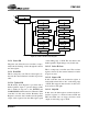
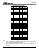
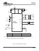
Table Of Contents
- Features
- Description
- 1. Pin Out - 144-Pin LQFP Package
- 2. Pin Out - 160-Ball FBGA Package
- 3. Pin Descriptions
- 4. operation
- 5. Power-up
- 6. Master Clock
- 7. G.772 Monitoring
- 8. Building Integrated Timing Systems (BITS) Clock Mode
- 9. Transmitter
- 10. Receiver
- 11. Jitter Attenuator
- 12. Operational Summary
- 13. Host Mode
- 14. Register Descriptions
- 14.1 Revision/IDcode Register (00h)
- 14.2 Analog Loopback Register (01h)
- 14.3 Remote Loopback Register (02h)
- 14.4 TAOS Enable Register (03h)
- 14.5 LOS Status Register (04h)
- 14.6 DFM Status Register (05h)
- 14.7 LOS Interrupt Enable Register (06h)
- 14.8 DFM Interrupt Enable Register (07h)
- 14.9 LOS Interrupt Status Register (08h)
- 14.10 DFM Interrupt Status Register (09h)
- 14.11 Software Reset Register (0Ah)
- 14.12 Performance Monitor Register (0Bh)
- 14.13 Digital Loopback Reset Register (0Ch)
- 14.14 LOS/AIS Mode Enable Register (0Dh)
- 14.15 Automatic TAOS Register (0Eh)
- 14.16 Global Control Register (0Fh)
- 14.17 Line Length Channel ID Register (10h)
- 14.18 Line Length Data Register (11h)
- 14.19 Output Disable Register (12h)
- 14.20 AIS Status Register (13h)
- 14.21 AIS Interrupt Enable Register (14h)
- 14.22 AIS Interrupt Status Register (15h)
- 14.23 AWG Broadcast Register (16h)
- 14.24 AWG Phase Address Register (17h)
- 14.25 AWG Phase Data Register (18h)
- 14.26 AWG Enable Register (19h)
- 14.27 Reserved Register (1Ah)
- 14.28 Reserved Register (1Bh)
- 14.29 Reserved Register (1Ch)
- 14.30 Reserved Register (1Dh)
- 14.31 Bits Clock Enable Register (1Eh)
- 14.32 Reserved Register (1Fh)
- 14.33 Status Registers
- 15. Arbitrary Waveform Generator
- 16. JTAG Support
- 17. Boundary Scan Register (BSR)
- 18. Applications
- 19. Characteristics and specifications
- 19.1 Absolute Maximum Ratings
- 19.2 Recommended Operating Conditions
- 19.3 Digital Characteristics
- 19.4 Transmitter Analog Characteristics
- 19.5 Receiver Analog Characteristics
- 19.6 Jitter Attenuator Characteristics
- 19.7 Master Clock Switching Characteristics
- 19.8 Transmit Switching Characteristics
- 19.9 Receive Switching Characteristics
- 19.10 Switching Characteristics - Serial Port
- 19.11 Switching Characteristics - Parallel Port (Multiplexed Mode)
- 19.12 Switching Characteristics- Parallel Port (Non-Multiplexed Mode)
- 19.13 Switching Characteristics - JTAG
- 20. Compliant Recommendations and specifications
- 21. 160-Ball FBGA package dimensions
- 22. 144-Pin LQFP Package dimensions

CS61880
DS450PP3 43
sample address (00000 binary) needs to be written
to the AWG Phase Address Register (17h) (See
Section 14.24 on page 39), and each subsequent ac-
cess (read or write) to the AWG Phase Data Reg-
ister (18h) (See Section 14.25 on page 39) will
automatically increment the phase sample address.
The channel address, however, remains unaffected
by the Auto-Increment mode. The AWG Phase
Address Register (17h) (See Section 14.24 on
page 39) needs to be re-written in order to re-start
the phase sample address sequence from the new
phase sample address.
The AWG Broadcast function allows the same data
to be written to multiple channels simultaneously.
This is done with the use of the AWG Broadcast
Register (16h) (See Section 14.23 on page 39),
each bit in the AWG Broadcast Register corre-
sponds to a different channel (e.g. bit 0 is channel
0, and bit 3 is channel 3 and etc.). To use the AWG
Broadcast function MCLK must be present. When
MCLK is inactive the AWG Broadcast function is
disabled.
To write the same pulse shaping data to multiple
channels, simple set the corresponding bit to “1” in
the AWG Broadcast Register (16h) (See Section
14.23 on page 39) before accessing the AWG
phase data register. This function only requires that
one of the eight channel addresses be written to the
AWG Phase Address Register (17h) (See Section
14.24 on page 39). During an AWG read sequence,
the bits in the AWG Broadcast Register are ig-
nored. During an AWG write sequence, the select-
ed channel or channels are specified by both the
channel address specified by the upper bits of the
AWG Phase Address Register (17h) (See Section
14.24 on page 39) and the selected channel or chan-
nels in the AWG Broadcast Register (16h) (See
Section 14.23 on page 39).
During a multiple channel write the first channel
that is written to, is the channel that was addressed
by the AWG Phase Address Register. This chan-
nel’s bit in the AWG Broadcast Register can be set
to either “1” or “0”.
For a more descriptive explanation of how to use
the AWG function refer to the Application Note
AN204, How To Use The CS61880/CS61884 Arbi-
trary Waveform Generator.
16. JTAG SUPPORT
The CS61880 supports the IEEE Boundary Scan
Specification as described in the IEEE 1149.1 stan-
dards. A Test Access Port (TAP) is provided that
consists of the TAP controller, the instruction reg-
ister (IR), by-pass register (BPR), device ID regis-
ter (IDR), the boundary scan register (BSR), and
the 5 standard pins (TRST, TCK, TMS, TDI, and
TDO). A block diagram of the test access port is
shown in Figure 14 on page 44. The test clock in-
put (TCK) is used to sample input data on TDI, and
shift output data through TDO. The TMS input is
used to step the TAP controller through its various
states.
The instruction register is used to select test execu-
tion or register access. The by-pass register pro-
vides a direct connection between the TDI input
and the TDO output. The device identification reg-
ister contains a 32-bit device identifier.
The Boundary Scan Register is used to support test-
ing of IC inter-connectivity. Using the Boundary
Scan Register, the digital input pins can be sampled
and shifted out on TDO. In addition, this register
can also be used to drive digital output pins to a
user defined state.