
User Manual
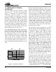
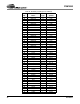
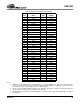
Table Of Contents
- Features
- Description
- 1. Pin Out - 144-Pin LQFP Package
- 2. Pin Out - 160-Ball FBGA Package
- 3. Pin Descriptions
- 4. operation
- 5. Power-up
- 6. Master Clock
- 7. G.772 Monitoring
- 8. Building Integrated Timing Systems (BITS) Clock Mode
- 9. Transmitter
- 10. Receiver
- 11. Jitter Attenuator
- 12. Operational Summary
- 13. Host Mode
- 14. Register Descriptions
- 14.1 Revision/IDcode Register (00h)
- 14.2 Analog Loopback Register (01h)
- 14.3 Remote Loopback Register (02h)
- 14.4 TAOS Enable Register (03h)
- 14.5 LOS Status Register (04h)
- 14.6 DFM Status Register (05h)
- 14.7 LOS Interrupt Enable Register (06h)
- 14.8 DFM Interrupt Enable Register (07h)
- 14.9 LOS Interrupt Status Register (08h)
- 14.10 DFM Interrupt Status Register (09h)
- 14.11 Software Reset Register (0Ah)
- 14.12 Performance Monitor Register (0Bh)
- 14.13 Digital Loopback Reset Register (0Ch)
- 14.14 LOS/AIS Mode Enable Register (0Dh)
- 14.15 Automatic TAOS Register (0Eh)
- 14.16 Global Control Register (0Fh)
- 14.17 Line Length Channel ID Register (10h)
- 14.18 Line Length Data Register (11h)
- 14.19 Output Disable Register (12h)
- 14.20 AIS Status Register (13h)
- 14.21 AIS Interrupt Enable Register (14h)
- 14.22 AIS Interrupt Status Register (15h)
- 14.23 AWG Broadcast Register (16h)
- 14.24 AWG Phase Address Register (17h)
- 14.25 AWG Phase Data Register (18h)
- 14.26 AWG Enable Register (19h)
- 14.27 Reserved Register (1Ah)
- 14.28 Reserved Register (1Bh)
- 14.29 Reserved Register (1Ch)
- 14.30 Reserved Register (1Dh)
- 14.31 Bits Clock Enable Register (1Eh)
- 14.32 Reserved Register (1Fh)
- 14.33 Status Registers
- 15. Arbitrary Waveform Generator
- 16. JTAG Support
- 17. Boundary Scan Register (BSR)
- 18. Applications
- 19. Characteristics and specifications
- 19.1 Absolute Maximum Ratings
- 19.2 Recommended Operating Conditions
- 19.3 Digital Characteristics
- 19.4 Transmitter Analog Characteristics
- 19.5 Receiver Analog Characteristics
- 19.6 Jitter Attenuator Characteristics
- 19.7 Master Clock Switching Characteristics
- 19.8 Transmit Switching Characteristics
- 19.9 Receive Switching Characteristics
- 19.10 Switching Characteristics - Serial Port
- 19.11 Switching Characteristics - Parallel Port (Multiplexed Mode)
- 19.12 Switching Characteristics- Parallel Port (Non-Multiplexed Mode)
- 19.13 Switching Characteristics - JTAG
- 20. Compliant Recommendations and specifications
- 21. 160-Ball FBGA package dimensions
- 22. 144-Pin LQFP Package dimensions

CS61880
42 DS450PP3
15. ARBITRARY WAVEFORM
GENERATOR
Using the Arbitrary Waveform Generator (AWG)
allows the user to customize the transmit pulse
shapes to compensate for nonstandard cables,
transformers, protection circuitry, or to reduce
power consumption by reducing the output pulse
amplitude. A channel is configured for a custom
pulse shape by enabling the AWG for that channel
and then storing data representing the pulse shape
into the 24 phase sample locations. Each channel
has a separate AWG, so all eight channels can have
a different customized pulse shape. The micropro-
cessor interface, is used to read from or write to the
AWG, while the device is in host mode.
In the AWG RAM, the pulse shape is divided into
two unit intervals (UI). There are 12 phase sample
addresses in each UI. The first UI is for the main
part of the pulse and the second UI is for the “tail”
of the pulse (Refer to Figure 13). A complete pulse-
shape is represented by 24 phase samples. Data
written in the first UI represents a valid pulse
shape, while data in the second UI must be set to
zero at all times. Writing values other that zero to
the second UI will cause the pulse shape to be in-
valid.
The data in each phase sample is a 7-bit two’s com-
plement number with a maximum positive value of
0x3f, and a maximum negative value of 0x40. The
terms “positive” and “negative” are defined for a
positive going pulse only. The pulse generation cir-
cuitry automatically inverts the pulse for negative
going pulses. The data stored in the lowest phase
address corresponds to the first phase sample that
will be transmitted in time. The typical voltage step
for each mode of operation is as follows: for E1
75 Ω mode the typical voltage step is 42 mV/LSB
and for E1 120 Ω mode the typical voltage step is
54 mV/LSB all voltage steps are measured across
the transformer secondary.
The following procedure describes how to enable
and write data into the AWG RAM to produce cus-
tomized pulse shapes to be transmitted for a specif-
ic channel or channels. First, enable the AWG
function for a specific channel or channels by writ-
ing a “1” to the corresponding bits in the AWG En-
able Register (19h) (See Section 14.26 on
page 40). When the corresponding bit or bits in the
AWG Enable Register are set to “0” pre-pro-
grammed pulse shapes are selected for transmis-
sion. Then the desired channel and phase sample
address must be written to the AWG Phase Ad-
dress Register (17h) (See Section 14.24 on
page 39). Once the channel and phase sample ad-
dress have been written, the actual phase sample
data may be entered into the AWG Phase Data
Register (18h) (See Section 14.25 on page 39) at
the selected phase sample address selected by the
lower five bits of the AWG Phase Address Regis-
ter (17h) (See Section 14.24 on page 39)).
To change the phase sample address of the selected
channel the user may use either of the following
steps. The user can re-write the phase sample ad-
dress to the AWG Phase Address Register or set the
Auto-Increment bit (Bit 7) in the Global Control
Register (0Fh) (See Section 14.16 on page 37) to
“1” before writing to the AWG Phase Data Regis-
ter. When this bit is set to “1” only the first phase
E1 AWG Example
U1 U2
Figure 13. Arbitrary Waveform UI