
User Manual


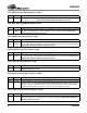
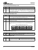
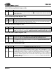
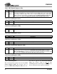
Table Of Contents
- Features
- Description
- 1. Pin Out - 144-Pin LQFP Package
- 2. Pin Out - 160-Ball FBGA Package
- 3. Pin Descriptions
- 4. operation
- 5. Power-up
- 6. Master Clock
- 7. G.772 Monitoring
- 8. Building Integrated Timing Systems (BITS) Clock Mode
- 9. Transmitter
- 10. Receiver
- 11. Jitter Attenuator
- 12. Operational Summary
- 13. Host Mode
- 14. Register Descriptions
- 14.1 Revision/IDcode Register (00h)
- 14.2 Analog Loopback Register (01h)
- 14.3 Remote Loopback Register (02h)
- 14.4 TAOS Enable Register (03h)
- 14.5 LOS Status Register (04h)
- 14.6 DFM Status Register (05h)
- 14.7 LOS Interrupt Enable Register (06h)
- 14.8 DFM Interrupt Enable Register (07h)
- 14.9 LOS Interrupt Status Register (08h)
- 14.10 DFM Interrupt Status Register (09h)
- 14.11 Software Reset Register (0Ah)
- 14.12 Performance Monitor Register (0Bh)
- 14.13 Digital Loopback Reset Register (0Ch)
- 14.14 LOS/AIS Mode Enable Register (0Dh)
- 14.15 Automatic TAOS Register (0Eh)
- 14.16 Global Control Register (0Fh)
- 14.17 Line Length Channel ID Register (10h)
- 14.18 Line Length Data Register (11h)
- 14.19 Output Disable Register (12h)
- 14.20 AIS Status Register (13h)
- 14.21 AIS Interrupt Enable Register (14h)
- 14.22 AIS Interrupt Status Register (15h)
- 14.23 AWG Broadcast Register (16h)
- 14.24 AWG Phase Address Register (17h)
- 14.25 AWG Phase Data Register (18h)
- 14.26 AWG Enable Register (19h)
- 14.27 Reserved Register (1Ah)
- 14.28 Reserved Register (1Bh)
- 14.29 Reserved Register (1Ch)
- 14.30 Reserved Register (1Dh)
- 14.31 Bits Clock Enable Register (1Eh)
- 14.32 Reserved Register (1Fh)
- 14.33 Status Registers
- 15. Arbitrary Waveform Generator
- 16. JTAG Support
- 17. Boundary Scan Register (BSR)
- 18. Applications
- 19. Characteristics and specifications
- 19.1 Absolute Maximum Ratings
- 19.2 Recommended Operating Conditions
- 19.3 Digital Characteristics
- 19.4 Transmitter Analog Characteristics
- 19.5 Receiver Analog Characteristics
- 19.6 Jitter Attenuator Characteristics
- 19.7 Master Clock Switching Characteristics
- 19.8 Transmit Switching Characteristics
- 19.9 Receive Switching Characteristics
- 19.10 Switching Characteristics - Serial Port
- 19.11 Switching Characteristics - Parallel Port (Multiplexed Mode)
- 19.12 Switching Characteristics- Parallel Port (Non-Multiplexed Mode)
- 19.13 Switching Characteristics - JTAG
- 20. Compliant Recommendations and specifications
- 21. 160-Ball FBGA package dimensions
- 22. 144-Pin LQFP Package dimensions
CS61880
DS450PP3 39
14.21 AIS Interrupt Enable Register (14h)
14.22 AIS Interrupt Status Register (15h)
14.23 AWG Broadcast Register (16h)
14.24 AWG Phase Address Register (17h)
14.25 AWG Phase Data Register (18h)
BIT NAME Description
[7:0] AISE 7-0 This register enables changes in the AIS Status register to be reflected in the AIS Interrupt
Status register, thus causing an interrupt on the INT
pin. Register bits default to 00h after
power-up or reset.
BIT NAME Description
[7:0] AISI 7-0
Bit n is set to “1” to indicate a change of status of bit n in the AIS Status Register. The bits in
this register indicate which channel changed in status since the last cleared AIS interrupt.
Register bits default to 00h after power-up or reset.
BIT NAME Description
[7:0] AWGB 7-0
Setting bit n to “1” causes the phase data in the AWG Phase Data Register to be written to
the corresponding channel or channels simultaneously. (Refer to Arbitrary Waveform Gen-
erator (See Section 15 on page 42). Register bits default to 00h after power-up or reset.
BIT NAME Description
[7:5] AWGA These bits specify the target channel 0-7. (Refer to Arbitrary Waveform Generator (See
Section 15 on page 42). Register bits default to 00h after power-up or reset.
[4:0] PA[4:0] These bits specify 1 of 24 phase sample address locations of the AWG, that the phase data
in the AWG Phase Data Register is written to or read from. Register bits default to 00h
after power-up or reset.
BIT NAME Description
[7] RSVD RESERVED (This bit must be set to 0.)
[6:0] AWGD [6:0]
These bits are used for the pulse shape data that will be written to or read from the AWG
phase location specified by the AWG Phase Address Register. The value written to or read
from this register will be written to or read from the AWG phase sample location specified by
the AWG Phase Address register. A software reset through the Software Reset Register
does not effect the contents of this register. The data in each phase is a 7-bit 2’s complement
number (the maximum positive value is 3Fh and the maximum negative value is 40h). (Refer
to Arbitrary Waveform Generator (See Section 15 on page 42). Register bits default to
00h after power-up.