
User Manual
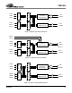
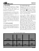

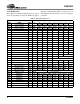

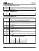
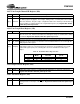
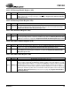
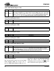
Table Of Contents
- Features
- Description
- 1. Pin Out - 144-Pin LQFP Package
- 2. Pin Out - 160-Ball FBGA Package
- 3. Pin Descriptions
- 4. operation
- 5. Power-up
- 6. Master Clock
- 7. G.772 Monitoring
- 8. Building Integrated Timing Systems (BITS) Clock Mode
- 9. Transmitter
- 10. Receiver
- 11. Jitter Attenuator
- 12. Operational Summary
- 13. Host Mode
- 14. Register Descriptions
- 14.1 Revision/IDcode Register (00h)
- 14.2 Analog Loopback Register (01h)
- 14.3 Remote Loopback Register (02h)
- 14.4 TAOS Enable Register (03h)
- 14.5 LOS Status Register (04h)
- 14.6 DFM Status Register (05h)
- 14.7 LOS Interrupt Enable Register (06h)
- 14.8 DFM Interrupt Enable Register (07h)
- 14.9 LOS Interrupt Status Register (08h)
- 14.10 DFM Interrupt Status Register (09h)
- 14.11 Software Reset Register (0Ah)
- 14.12 Performance Monitor Register (0Bh)
- 14.13 Digital Loopback Reset Register (0Ch)
- 14.14 LOS/AIS Mode Enable Register (0Dh)
- 14.15 Automatic TAOS Register (0Eh)
- 14.16 Global Control Register (0Fh)
- 14.17 Line Length Channel ID Register (10h)
- 14.18 Line Length Data Register (11h)
- 14.19 Output Disable Register (12h)
- 14.20 AIS Status Register (13h)
- 14.21 AIS Interrupt Enable Register (14h)
- 14.22 AIS Interrupt Status Register (15h)
- 14.23 AWG Broadcast Register (16h)
- 14.24 AWG Phase Address Register (17h)
- 14.25 AWG Phase Data Register (18h)
- 14.26 AWG Enable Register (19h)
- 14.27 Reserved Register (1Ah)
- 14.28 Reserved Register (1Bh)
- 14.29 Reserved Register (1Ch)
- 14.30 Reserved Register (1Dh)
- 14.31 Bits Clock Enable Register (1Eh)
- 14.32 Reserved Register (1Fh)
- 14.33 Status Registers
- 15. Arbitrary Waveform Generator
- 16. JTAG Support
- 17. Boundary Scan Register (BSR)
- 18. Applications
- 19. Characteristics and specifications
- 19.1 Absolute Maximum Ratings
- 19.2 Recommended Operating Conditions
- 19.3 Digital Characteristics
- 19.4 Transmitter Analog Characteristics
- 19.5 Receiver Analog Characteristics
- 19.6 Jitter Attenuator Characteristics
- 19.7 Master Clock Switching Characteristics
- 19.8 Transmit Switching Characteristics
- 19.9 Receive Switching Characteristics
- 19.10 Switching Characteristics - Serial Port
- 19.11 Switching Characteristics - Parallel Port (Multiplexed Mode)
- 19.12 Switching Characteristics- Parallel Port (Non-Multiplexed Mode)
- 19.13 Switching Characteristics - JTAG
- 20. Compliant Recommendations and specifications
- 21. 160-Ball FBGA package dimensions
- 22. 144-Pin LQFP Package dimensions
CS61880
38 DS450PP3
14.17 Line Length Channel ID Register (10h)
14.18 Line Length Data Register (11h)
14.19 Output Disable Register (12h)
14.20 AIS Status Register (13h)
BIT NAME Description
[7:3] RSVD 7-3 RESERVED (These bits must be set to 0.)
[2:0] LLID 2-0
The value written to these bits specify the LIU channel for which the Pulse Shape Configura-
tion Data (register 11h) applies. For example, writing a value of a binary 000 to the 3-LSBs
will select channel 0. The pulse shape configuration data for the channel specified in this reg-
ister are written or read through the Line Length Data Register (11h). Register bits default
to 00h after power-up or reset.
BIT NAME Description
The value written to the 4-LSBs of this register specifies whether the device is operating in
either E1 75 Ω or E1 120 Ω mode and the associated pulse shape as shown below is being
transmitted. Register bits default to 00h after power-up or reset.
[7:5] RSVD RESERVED (These bits must be set to 0.)
[4] INT_EXTB
This bit specifies the use of internal (Int_ExtB = 1) or external (Int_ExtB = 0) receiver line
matching. The line impedance for both the receiver and transmitter are chosen through the
LEN [3:0] bits in this register.
[3:0] LEN[3:0]
These bits set the line impedance for both the receiver and the transmitter path and the
desired pulse shape for a specific channel. The channel is selected with the Line Length
Channel ID register (0x10). The following table shows the available transmitter pulse
shapes.
BIT NAME Description
[7:0] OENB 7-0 Setting bit n of this register to “1” High-Z the TX output driver on channel n of the device.
Register bits default to 00h after power-up or reset.
BIT NAME Description
[7:0] AISS 7-0 A “1” in bit position n indicates that the receiver has detected an AIS condition on channel n,
which generates an interrupt on the INT
pin. Register bits default to 00h after power-up or
reset.
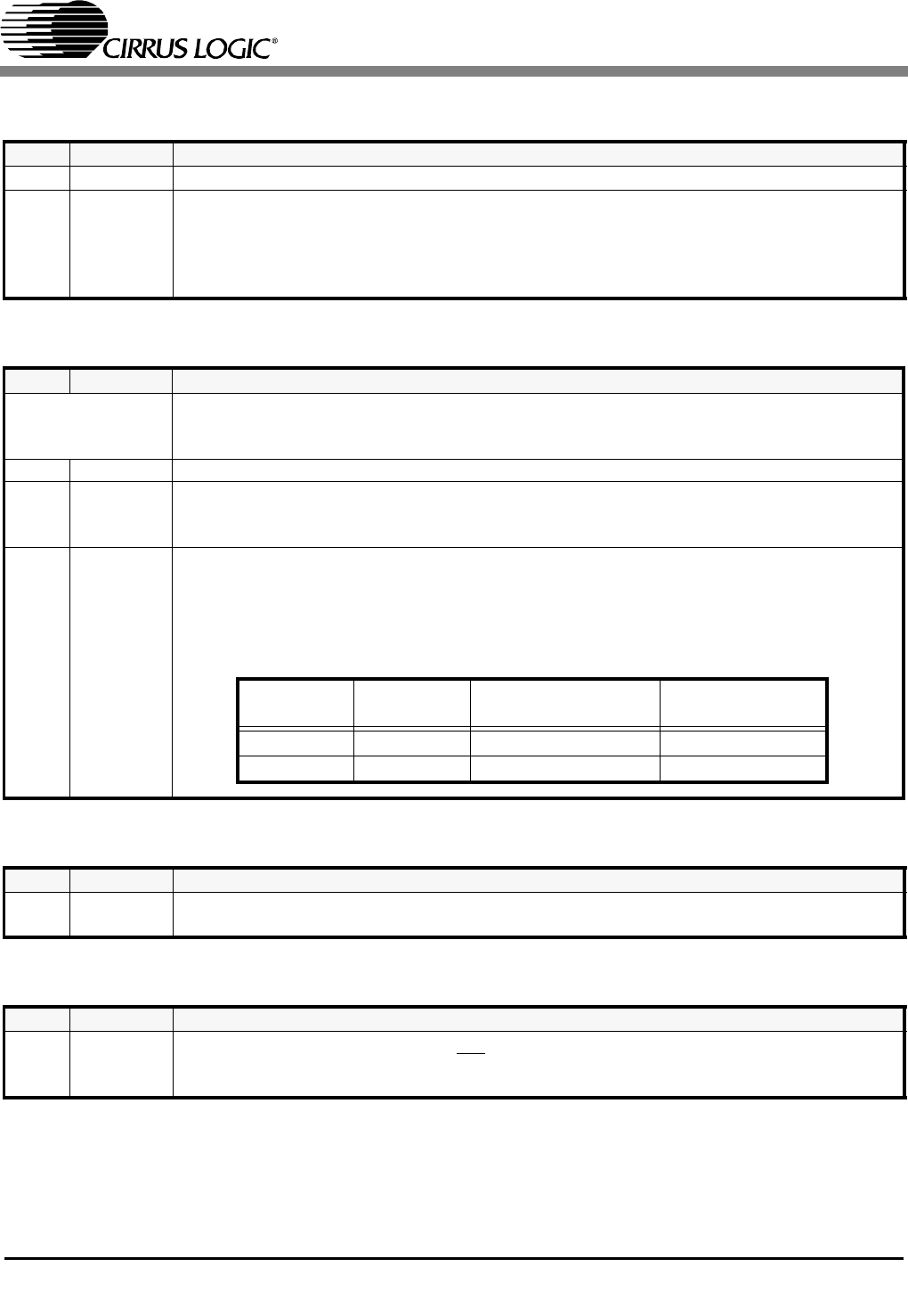
Table 12. Transmitter Pulse Shape Selection
LEN [3:0] Operation
Mode
Line Length
Selection
Phase Samples
per UI
0000 E1 120 Ω 3.0 V 12
1000 E1 75 Ω 2.37 V 12