
User Manual


Table Of Contents
- Features
- Description
- 1. Pin Out - 144-Pin LQFP Package
- 2. Pin Out - 160-Ball FBGA Package
- 3. Pin Descriptions
- 4. operation
- 5. Power-up
- 6. Master Clock
- 7. G.772 Monitoring
- 8. Building Integrated Timing Systems (BITS) Clock Mode
- 9. Transmitter
- 10. Receiver
- 11. Jitter Attenuator
- 12. Operational Summary
- 13. Host Mode
- 14. Register Descriptions
- 14.1 Revision/IDcode Register (00h)
- 14.2 Analog Loopback Register (01h)
- 14.3 Remote Loopback Register (02h)
- 14.4 TAOS Enable Register (03h)
- 14.5 LOS Status Register (04h)
- 14.6 DFM Status Register (05h)
- 14.7 LOS Interrupt Enable Register (06h)
- 14.8 DFM Interrupt Enable Register (07h)
- 14.9 LOS Interrupt Status Register (08h)
- 14.10 DFM Interrupt Status Register (09h)
- 14.11 Software Reset Register (0Ah)
- 14.12 Performance Monitor Register (0Bh)
- 14.13 Digital Loopback Reset Register (0Ch)
- 14.14 LOS/AIS Mode Enable Register (0Dh)
- 14.15 Automatic TAOS Register (0Eh)
- 14.16 Global Control Register (0Fh)
- 14.17 Line Length Channel ID Register (10h)
- 14.18 Line Length Data Register (11h)
- 14.19 Output Disable Register (12h)
- 14.20 AIS Status Register (13h)
- 14.21 AIS Interrupt Enable Register (14h)
- 14.22 AIS Interrupt Status Register (15h)
- 14.23 AWG Broadcast Register (16h)
- 14.24 AWG Phase Address Register (17h)
- 14.25 AWG Phase Data Register (18h)
- 14.26 AWG Enable Register (19h)
- 14.27 Reserved Register (1Ah)
- 14.28 Reserved Register (1Bh)
- 14.29 Reserved Register (1Ch)
- 14.30 Reserved Register (1Dh)
- 14.31 Bits Clock Enable Register (1Eh)
- 14.32 Reserved Register (1Fh)
- 14.33 Status Registers
- 15. Arbitrary Waveform Generator
- 16. JTAG Support
- 17. Boundary Scan Register (BSR)
- 18. Applications
- 19. Characteristics and specifications
- 19.1 Absolute Maximum Ratings
- 19.2 Recommended Operating Conditions
- 19.3 Digital Characteristics
- 19.4 Transmitter Analog Characteristics
- 19.5 Receiver Analog Characteristics
- 19.6 Jitter Attenuator Characteristics
- 19.7 Master Clock Switching Characteristics
- 19.8 Transmit Switching Characteristics
- 19.9 Receive Switching Characteristics
- 19.10 Switching Characteristics - Serial Port
- 19.11 Switching Characteristics - Parallel Port (Multiplexed Mode)
- 19.12 Switching Characteristics- Parallel Port (Non-Multiplexed Mode)
- 19.13 Switching Characteristics - JTAG
- 20. Compliant Recommendations and specifications
- 21. 160-Ball FBGA package dimensions
- 22. 144-Pin LQFP Package dimensions
CS61880
DS450PP3 33
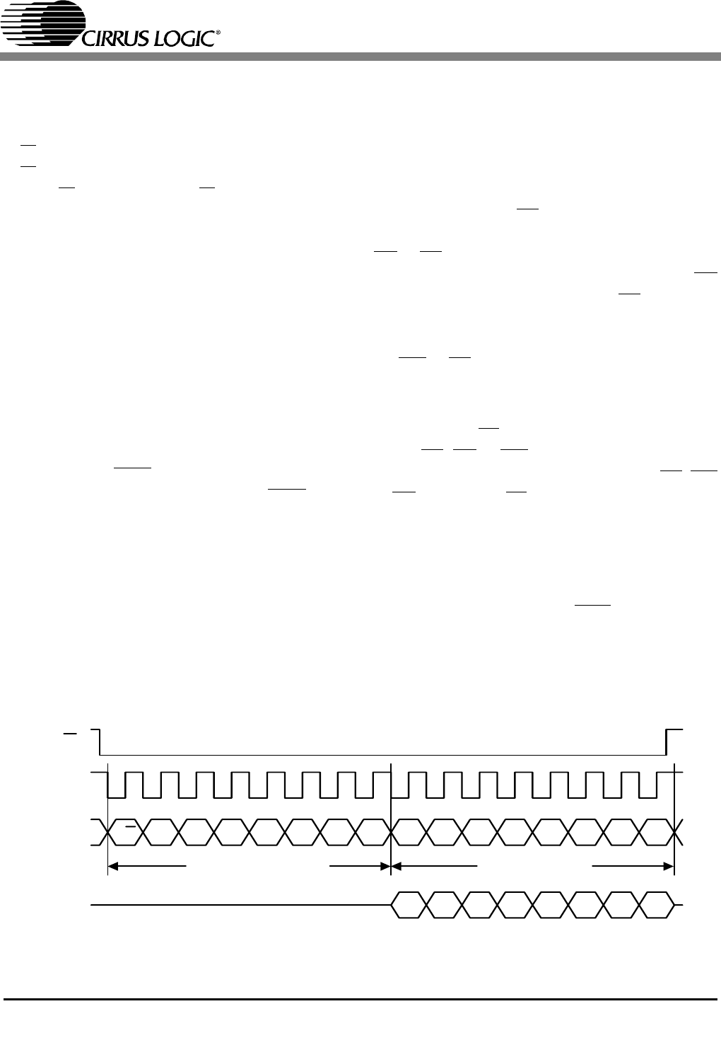
bidirectional I/O port, SDI and SDO may be tied to-
gether.
As illustrated in Figure 12, the ACB consists of a
R/W bit, address field, and two reserved bits. The
R/W bit specifies if the current register access is a
read (R/W = 1) or a write (R/W = 0) operation. The
address field specifies the register address from
0x00 to 0x1f.
13.3 Parallel Port Operation
Parallel port host mode operation is selected when
the MODE pin is high. In this mode, the CS61880
register set is accessed using an 8-bit, multiplexed
bidirectional address/data bus D[7:0]. Timing over
the parallel port is independent of the transmit and
receive system timing.
The device is compatible with both Intel and Mo-
torola bus formats. The Intel bus format is selected
when the INTL/MOT pin is high and the Motorola
bus format is selected when the INTL/MOT pin is
low. In either mode, the interface can have the ad-
dress and data multiplexed over the same 8-bit bus
or on separate busses. This operation is controlled
with the MUX pin; MUX = 1 means that the paral-
lel port has its address and data multiplexed over
the same bus; MUX = 0 defines a non-multiplexed
bus. The timing for the different modes are shown
in Figure 28, Figure 26, Figure 25, Figure 27,
Figure 29, Figure 30, Figure 31 and Figure 32.
Multiplexed Intel and Motorola modes are shown
in Figure 28, Figure 26, Figure 25 and Figure 27. A
read or write is initiated by writing an address byte
to D[7:0]. The device latches the address on the
falling edge of ALE(AS). During a read cycle, the
register data is output during the later portion of the
RD or DS pulses. The read cycle is terminated and
the bus returns to a high impedance state as RD
transitions high in Intel timing or DS transitions
high in Motorola timing. During a write cycle, val-
id write data must be present and held stable during
the WR or DS pulses.
Non-multiplexed Intel and Motorola modes are
shown in Figure 29, Figure 30, Figure 32 and
Figure 31. The CS pin initiates the cycle, followed
by the DS, RD or WR pin. Data is latched into or
out of the part using the rising edge of the DS, WR
or RD pin. Raising CS ends the cycle.
In Intel mode, the RDY output pin is normally in a
high impedance state; it pulses low once to ac-
knowledge that the chip has been selected, and high
again to acknowledge that data has been written or
read. In Motorola mode, the ACK pin performs a
similar function; it drives high to indicate that the
address has been received by the part, and goes low
again to indicate that data has been written or read.
CS
SDI
SCLK
SDO
CLKE=0
0
R/W
000 001D0D1D2D5D3 D6D4 D7
D0 D1 D2 D5D3 D6D4 D7
Address/Command Byte Data Input/Output
Figure 12. Serial Read/Write Format (SPOL = 0)