
User Manual
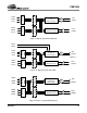


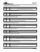
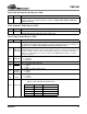
Table Of Contents
- Features
- Description
- 1. Pin Out - 144-Pin LQFP Package
- 2. Pin Out - 160-Ball FBGA Package
- 3. Pin Descriptions
- 4. operation
- 5. Power-up
- 6. Master Clock
- 7. G.772 Monitoring
- 8. Building Integrated Timing Systems (BITS) Clock Mode
- 9. Transmitter
- 10. Receiver
- 11. Jitter Attenuator
- 12. Operational Summary
- 13. Host Mode
- 14. Register Descriptions
- 14.1 Revision/IDcode Register (00h)
- 14.2 Analog Loopback Register (01h)
- 14.3 Remote Loopback Register (02h)
- 14.4 TAOS Enable Register (03h)
- 14.5 LOS Status Register (04h)
- 14.6 DFM Status Register (05h)
- 14.7 LOS Interrupt Enable Register (06h)
- 14.8 DFM Interrupt Enable Register (07h)
- 14.9 LOS Interrupt Status Register (08h)
- 14.10 DFM Interrupt Status Register (09h)
- 14.11 Software Reset Register (0Ah)
- 14.12 Performance Monitor Register (0Bh)
- 14.13 Digital Loopback Reset Register (0Ch)
- 14.14 LOS/AIS Mode Enable Register (0Dh)
- 14.15 Automatic TAOS Register (0Eh)
- 14.16 Global Control Register (0Fh)
- 14.17 Line Length Channel ID Register (10h)
- 14.18 Line Length Data Register (11h)
- 14.19 Output Disable Register (12h)
- 14.20 AIS Status Register (13h)
- 14.21 AIS Interrupt Enable Register (14h)
- 14.22 AIS Interrupt Status Register (15h)
- 14.23 AWG Broadcast Register (16h)
- 14.24 AWG Phase Address Register (17h)
- 14.25 AWG Phase Data Register (18h)
- 14.26 AWG Enable Register (19h)
- 14.27 Reserved Register (1Ah)
- 14.28 Reserved Register (1Bh)
- 14.29 Reserved Register (1Ch)
- 14.30 Reserved Register (1Dh)
- 14.31 Bits Clock Enable Register (1Eh)
- 14.32 Reserved Register (1Fh)
- 14.33 Status Registers
- 15. Arbitrary Waveform Generator
- 16. JTAG Support
- 17. Boundary Scan Register (BSR)
- 18. Applications
- 19. Characteristics and specifications
- 19.1 Absolute Maximum Ratings
- 19.2 Recommended Operating Conditions
- 19.3 Digital Characteristics
- 19.4 Transmitter Analog Characteristics
- 19.5 Receiver Analog Characteristics
- 19.6 Jitter Attenuator Characteristics
- 19.7 Master Clock Switching Characteristics
- 19.8 Transmit Switching Characteristics
- 19.9 Receive Switching Characteristics
- 19.10 Switching Characteristics - Serial Port
- 19.11 Switching Characteristics - Parallel Port (Multiplexed Mode)
- 19.12 Switching Characteristics- Parallel Port (Non-Multiplexed Mode)
- 19.13 Switching Characteristics - JTAG
- 20. Compliant Recommendations and specifications
- 21. 160-Ball FBGA package dimensions
- 22. 144-Pin LQFP Package dimensions
CS61880
32 DS450PP3
13. HOST MODE
Host mode allows the CS61880 to be configured
and monitored using an internal register set. (Refer
to Table 1, “Operation Mode Selection,” on
page 10). The term, “Host mode” applies to both
Parallel Host and Serial Host modes.
All of the internal registers are available in both Se-
rial and Parallel Host mode; the only difference is
in the functions of the interface pins, which are de-
scribed in Table 9 on page 32.
Serial port operation is compatible with the serial
ports of most microcontrollers. Parallel port opera-
tion can be configured to be compatible with 8-bit
microcontrollers from Motorola or Intel, with both
multiplexed or non-multiplexed address/data bus-
ses. (Refer to Table 10 on page 34 for host mode
registers).
13.1 SOFTWARE RESET
A software reset can be forced by writing the Soft-
ware Reset Register (0Ah) (See Section 14.11 on
page 36). A software reset initializes all registers to
their default settings and initializes all internal state
machines.
13.2 Serial Port Operation
Serial port host mode operation is selected when
the MODE pin is left open or set to VCC/2. In this
mode, the CS61880 register set is accessed by set-
ting the chip select (CS) pin low and communicat-
ing over the SDI, SDO, and SCLK pins. Timing
over the serial port is independent of the transmit
and receive system timing. Figure 12 illustrates the
format of serial port data transfers.
A read or write is initiated by writing an ad-
dress/command byte (ACB) to SDI. Only the
ADR0-ADR4 bits are valid; bits ADR5-ADR6 are
do not cares. During a read cycle, the register data
addressed by the ACB is output on SDO on the next
eight SCLK clock cycles. During a write cycle, the
data byte immediately follows the ACB.
Data is written to and read from the serial port in
LSB first format. When writing to the port, SDI
data is sampled by the device on the rising edge of
SCLK. The valid clock edge of the data on SDO is
controlled by the CLKE pin. When CLKE is low,
data on SDO is valid on the falling edge of SCLK.
When CLKE is high, data on SDO is valid on the
raising edge of SCLK. The SDO pin is High-Z
when not transmitting. If the host processor has a
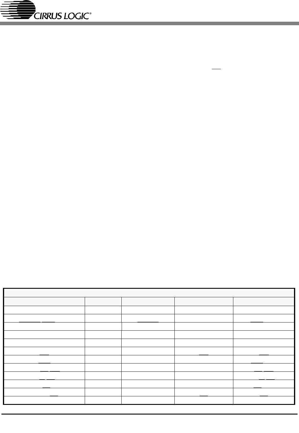
Table 9. Host Control Signal Descriptions
HOST CONTROL SIGNAL DESCRIPTIONS
PIN NAME PIN # HARDWARE SERIAL PARALLEL
MODE 11 LOW VDD/2 HIGH
MUX 43 BITSEN0 - MUX
CODEN
/MOT/INTL88CODEN -MOT/INTL
ADDR [4] 12 GND - ADDR[4]
ADDR[3:0] 13-16 ADDR[3:0] - ADDR [3:0]
LOOP[7:0], DATA[7:0] 28-21 LOOP[7:0] - DATA[7:0]
INT
82 Pulled Up INT INT
SDO/ACK/RDY 83 NC SDO ACK/RDY
SDI/DS
/WR 84 GND SDI DS/WR
R/W/RD 85 GND - R/W/RD
SCLK/AS/ALE 86 GND SCLK AS/ALE
JASEL/CS
87 JASEL CS CS