
User Manual
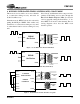
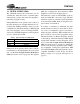
Table Of Contents
- Features
- Description
- 1. Pin Out - 144-Pin LQFP Package
- 2. Pin Out - 160-Ball FBGA Package
- 3. Pin Descriptions
- 4. operation
- 5. Power-up
- 6. Master Clock
- 7. G.772 Monitoring
- 8. Building Integrated Timing Systems (BITS) Clock Mode
- 9. Transmitter
- 10. Receiver
- 11. Jitter Attenuator
- 12. Operational Summary
- 13. Host Mode
- 14. Register Descriptions
- 14.1 Revision/IDcode Register (00h)
- 14.2 Analog Loopback Register (01h)
- 14.3 Remote Loopback Register (02h)
- 14.4 TAOS Enable Register (03h)
- 14.5 LOS Status Register (04h)
- 14.6 DFM Status Register (05h)
- 14.7 LOS Interrupt Enable Register (06h)
- 14.8 DFM Interrupt Enable Register (07h)
- 14.9 LOS Interrupt Status Register (08h)
- 14.10 DFM Interrupt Status Register (09h)
- 14.11 Software Reset Register (0Ah)
- 14.12 Performance Monitor Register (0Bh)
- 14.13 Digital Loopback Reset Register (0Ch)
- 14.14 LOS/AIS Mode Enable Register (0Dh)
- 14.15 Automatic TAOS Register (0Eh)
- 14.16 Global Control Register (0Fh)
- 14.17 Line Length Channel ID Register (10h)
- 14.18 Line Length Data Register (11h)
- 14.19 Output Disable Register (12h)
- 14.20 AIS Status Register (13h)
- 14.21 AIS Interrupt Enable Register (14h)
- 14.22 AIS Interrupt Status Register (15h)
- 14.23 AWG Broadcast Register (16h)
- 14.24 AWG Phase Address Register (17h)
- 14.25 AWG Phase Data Register (18h)
- 14.26 AWG Enable Register (19h)
- 14.27 Reserved Register (1Ah)
- 14.28 Reserved Register (1Bh)
- 14.29 Reserved Register (1Ch)
- 14.30 Reserved Register (1Dh)
- 14.31 Bits Clock Enable Register (1Eh)
- 14.32 Reserved Register (1Fh)
- 14.33 Status Registers
- 15. Arbitrary Waveform Generator
- 16. JTAG Support
- 17. Boundary Scan Register (BSR)
- 18. Applications
- 19. Characteristics and specifications
- 19.1 Absolute Maximum Ratings
- 19.2 Recommended Operating Conditions
- 19.3 Digital Characteristics
- 19.4 Transmitter Analog Characteristics
- 19.5 Receiver Analog Characteristics
- 19.6 Jitter Attenuator Characteristics
- 19.7 Master Clock Switching Characteristics
- 19.8 Transmit Switching Characteristics
- 19.9 Receive Switching Characteristics
- 19.10 Switching Characteristics - Serial Port
- 19.11 Switching Characteristics - Parallel Port (Multiplexed Mode)
- 19.12 Switching Characteristics- Parallel Port (Non-Multiplexed Mode)
- 19.13 Switching Characteristics - JTAG
- 20. Compliant Recommendations and specifications
- 21. 160-Ball FBGA package dimensions
- 22. 144-Pin LQFP Package dimensions
CS61880
30 DS450PP3
12.3 Digital Loopback
Digital Loopback causes the TCLK, TPOS, and
TNEG (or TDATA) inputs to be looped back
through the jitter attenuator (if enabled) to the
RCLK, RPOS, and RNEG (or RDATA) outputs.
The receive line interface is ignored, but data at
TPOS and TNEG (or TDATA) continues to be
transmitted to the line interface at TTIP and
TRING (Refer to Figure 9 on page 31).
Digital Loopback is only available during host
mode. It is selected using the appropriate bit in the
Digital Loopback Reset Register (0Ch) (See Sec-
tion 14.13 on page 36).
NOTE: TAOS can also be used during the Digital Loop-
back operation for the selected channel (Refer
to Figure 10 on page 31).
12.4 Remote Loopback
In remote loopback, the RPOS/RNEG and RCLK
outputs are internally input to the transmit circuits
for output on TTIP/TRING. In this mode the
TCLK, TPOS and TNEG inputs are ignored. (Refer
to Figure 11 on page 31). In hardware mode, Re-
mote Loopback is selected by driving the LOOP
pin for a certain channel low. In host mode, Remote
Loopback is selected for a given channel by writing
a one to the appropriate bit in the Remote Loop-
back Register (02h) (See Section 14.3 on
page 35).
NOTE: In hardware mode, Remote Loopback over-
rides TAOS for the selected channel. In host
mode, TAOS overrides Remote Loopback.
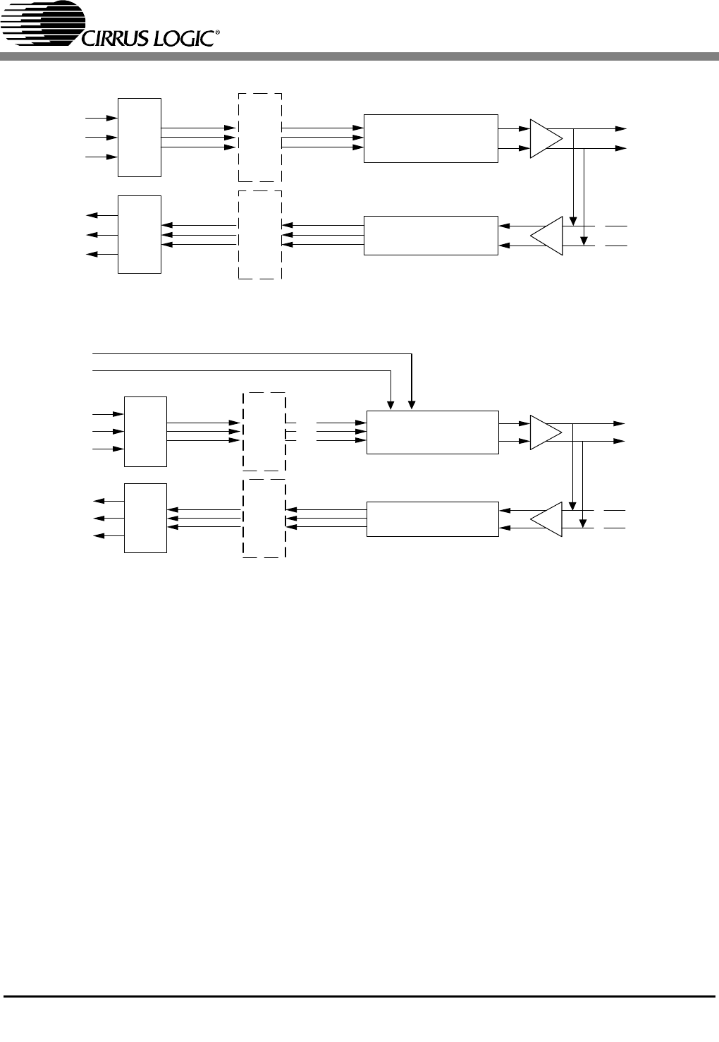
EncoderDecoder
TTIP
TRING
RTIP
RRING
TNEG
TCLK
RNEG
RCLK
TPOS
RPOS
Clock Recovery &
Data Recovery
Transmit
Control &
Pulse Shaper
Jitter
Attenuator
Jitter
Attenuator
Figure 7. Analog Loopback Block Diagram
EncoderDecoder
TNEG
TCLK
RNEG
RCLK
TPOS
RPOS
TAOS
MCLK
(All One's)
TTIP
TRING
RTIP
RRING
Clock Recovery &
Data Recovery
Transmit
Control &
Pulse Shaper
Jitter
Attenuator
Jitter
Attenuator
Figure 8. Analog Loopback with TAOS Block Diagram