
User Manual
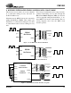
Table Of Contents
- Features
- Description
- 1. Pin Out - 144-Pin LQFP Package
- 2. Pin Out - 160-Ball FBGA Package
- 3. Pin Descriptions
- 4. operation
- 5. Power-up
- 6. Master Clock
- 7. G.772 Monitoring
- 8. Building Integrated Timing Systems (BITS) Clock Mode
- 9. Transmitter
- 10. Receiver
- 11. Jitter Attenuator
- 12. Operational Summary
- 13. Host Mode
- 14. Register Descriptions
- 14.1 Revision/IDcode Register (00h)
- 14.2 Analog Loopback Register (01h)
- 14.3 Remote Loopback Register (02h)
- 14.4 TAOS Enable Register (03h)
- 14.5 LOS Status Register (04h)
- 14.6 DFM Status Register (05h)
- 14.7 LOS Interrupt Enable Register (06h)
- 14.8 DFM Interrupt Enable Register (07h)
- 14.9 LOS Interrupt Status Register (08h)
- 14.10 DFM Interrupt Status Register (09h)
- 14.11 Software Reset Register (0Ah)
- 14.12 Performance Monitor Register (0Bh)
- 14.13 Digital Loopback Reset Register (0Ch)
- 14.14 LOS/AIS Mode Enable Register (0Dh)
- 14.15 Automatic TAOS Register (0Eh)
- 14.16 Global Control Register (0Fh)
- 14.17 Line Length Channel ID Register (10h)
- 14.18 Line Length Data Register (11h)
- 14.19 Output Disable Register (12h)
- 14.20 AIS Status Register (13h)
- 14.21 AIS Interrupt Enable Register (14h)
- 14.22 AIS Interrupt Status Register (15h)
- 14.23 AWG Broadcast Register (16h)
- 14.24 AWG Phase Address Register (17h)
- 14.25 AWG Phase Data Register (18h)
- 14.26 AWG Enable Register (19h)
- 14.27 Reserved Register (1Ah)
- 14.28 Reserved Register (1Bh)
- 14.29 Reserved Register (1Ch)
- 14.30 Reserved Register (1Dh)
- 14.31 Bits Clock Enable Register (1Eh)
- 14.32 Reserved Register (1Fh)
- 14.33 Status Registers
- 15. Arbitrary Waveform Generator
- 16. JTAG Support
- 17. Boundary Scan Register (BSR)
- 18. Applications
- 19. Characteristics and specifications
- 19.1 Absolute Maximum Ratings
- 19.2 Recommended Operating Conditions
- 19.3 Digital Characteristics
- 19.4 Transmitter Analog Characteristics
- 19.5 Receiver Analog Characteristics
- 19.6 Jitter Attenuator Characteristics
- 19.7 Master Clock Switching Characteristics
- 19.8 Transmit Switching Characteristics
- 19.9 Receive Switching Characteristics
- 19.10 Switching Characteristics - Serial Port
- 19.11 Switching Characteristics - Parallel Port (Multiplexed Mode)
- 19.12 Switching Characteristics- Parallel Port (Non-Multiplexed Mode)
- 19.13 Switching Characteristics - JTAG
- 20. Compliant Recommendations and specifications
- 21. 160-Ball FBGA package dimensions
- 22. 144-Pin LQFP Package dimensions

CS61880
DS450PP3 27
10.4 Receiver Powerdown/High-Z
All eight receivers are powered down when MCLK
is held low. In addition, this will force the RCLK,
RPOS/RDATA and RNEG outputs into a high im-
pedance state.
10.5 Loss-of-Signal (LOS)
The CS61880 makes use of both analog and digital
LOS detection circuitry that is compliant to the lat-
est specifications. The LOS condition can be set to
either ITU G.775 or ETSI 300 233. This change is
done through the LOS/AIS Mode Enable Regis-
ter (0Dh) (See Section 14.14 on page 37).
The LOS detector increments a counter each time a
zero is received, and resets the counter each time a
one “mark” is received. Depending on LOS detec-
tion mode, the LOS signal is set when a certain
number of consecutive zeros are received. In
Clock/Data recovery mode, this forces the recov-
ered clock to be replaced by MCLK at the RCLK
output. In addition the RPOS/RDATA and RNEG
outputs remain active for the length of the LOS pe-
riod, except when local and analog loopbacks are
enabled. Upon exiting LOS, the recovered clock re-
places MCLK on the RCLK output. In Data recov-
ery mode, RCLK is not replaced by MCLK when
LOS is active. The LOS detection modes are sum-
marized below.
NOTE: G.775 and ETSI 300 233 are both available in
host mode, but in hardware mode only ETSI
300 233 is available.
ITU G.775 (E1 Mode Only) - LOS is declared
when the received signal level is less than 200 mV
for 32 consecutive pulse periods (typical). The de-
vice exits LOS when the received signal achieves
12.5% ones density with no more than 15 consecu-
tive zeros in a 32-bit sliding window and the signal
level exceeds 250 mV.
ETSI 300 233 (E1 Host Mode Only) - The LOS
indicator becomes active when the receive signal
level drops below 200 mV for more than 2048
pulse periods (1 ms). The channel exits the LOS
state when the input signal exceeds 250 mV and
has transitions for more than 32 pulse periods
(16 µs). This LOS detection method can only be se-
lected while in host mode.
During host mode operation, LOS is reported in the
LOS Status Monitor Register. Both the LOS pins
and the register bits reflect LOS status in host mode
operation. The LOS pins and status bits are set high
(indicating loss of signal) during reset, power-up,
or channel powered-down.
10.6 Alarm Indication Signal (AIS)
The CS61880 detects all ones alarm condition per
the relevant ITU, and ETSI specifications. In gen-
eral, AIS is indicated when the one’s density of the
receive signal exceeds that dictated by the relevant
specification. This feature is only available in host
mode (Refer to LOS/AIS Mode Enable Register
(0Dh) (See Section 14.14 on page 37)).
ITU G.775 AIS (E1 Mode) - The AIS condition is
declared when less than 3 zeros are received within
two consecutive 512-bit windows. The AIS condi-
tion is cleared when 3 or more zeros are received in
two consecutive 512-bit windows.
ETSI 300 233 (E1 Mode) - The AIS condition is
declared when less than 3 zeros are received in a
512-bit window. The AIS condition is cleared
when a 512-bit window is received containing 3 or
more zeros.