
User Manual
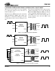
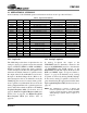
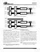
Table Of Contents
- Features
- Description
- 1. Pin Out - 144-Pin LQFP Package
- 2. Pin Out - 160-Ball FBGA Package
- 3. Pin Descriptions
- 4. operation
- 5. Power-up
- 6. Master Clock
- 7. G.772 Monitoring
- 8. Building Integrated Timing Systems (BITS) Clock Mode
- 9. Transmitter
- 10. Receiver
- 11. Jitter Attenuator
- 12. Operational Summary
- 13. Host Mode
- 14. Register Descriptions
- 14.1 Revision/IDcode Register (00h)
- 14.2 Analog Loopback Register (01h)
- 14.3 Remote Loopback Register (02h)
- 14.4 TAOS Enable Register (03h)
- 14.5 LOS Status Register (04h)
- 14.6 DFM Status Register (05h)
- 14.7 LOS Interrupt Enable Register (06h)
- 14.8 DFM Interrupt Enable Register (07h)
- 14.9 LOS Interrupt Status Register (08h)
- 14.10 DFM Interrupt Status Register (09h)
- 14.11 Software Reset Register (0Ah)
- 14.12 Performance Monitor Register (0Bh)
- 14.13 Digital Loopback Reset Register (0Ch)
- 14.14 LOS/AIS Mode Enable Register (0Dh)
- 14.15 Automatic TAOS Register (0Eh)
- 14.16 Global Control Register (0Fh)
- 14.17 Line Length Channel ID Register (10h)
- 14.18 Line Length Data Register (11h)
- 14.19 Output Disable Register (12h)
- 14.20 AIS Status Register (13h)
- 14.21 AIS Interrupt Enable Register (14h)
- 14.22 AIS Interrupt Status Register (15h)
- 14.23 AWG Broadcast Register (16h)
- 14.24 AWG Phase Address Register (17h)
- 14.25 AWG Phase Data Register (18h)
- 14.26 AWG Enable Register (19h)
- 14.27 Reserved Register (1Ah)
- 14.28 Reserved Register (1Bh)
- 14.29 Reserved Register (1Ch)
- 14.30 Reserved Register (1Dh)
- 14.31 Bits Clock Enable Register (1Eh)
- 14.32 Reserved Register (1Fh)
- 14.33 Status Registers
- 15. Arbitrary Waveform Generator
- 16. JTAG Support
- 17. Boundary Scan Register (BSR)
- 18. Applications
- 19. Characteristics and specifications
- 19.1 Absolute Maximum Ratings
- 19.2 Recommended Operating Conditions
- 19.3 Digital Characteristics
- 19.4 Transmitter Analog Characteristics
- 19.5 Receiver Analog Characteristics
- 19.6 Jitter Attenuator Characteristics
- 19.7 Master Clock Switching Characteristics
- 19.8 Transmit Switching Characteristics
- 19.9 Receive Switching Characteristics
- 19.10 Switching Characteristics - Serial Port
- 19.11 Switching Characteristics - Parallel Port (Multiplexed Mode)
- 19.12 Switching Characteristics- Parallel Port (Non-Multiplexed Mode)
- 19.13 Switching Characteristics - JTAG
- 20. Compliant Recommendations and specifications
- 21. 160-Ball FBGA package dimensions
- 22. 144-Pin LQFP Package dimensions

CS61880
26 DS450PP3
10. RECEIVER
The CS61880 contains eight identical receivers that
utilize an internal matched impedance technique
that provides for the use of a common set of exter-
nal components for 120 Ω (E1), and 75 Ω (Ε1) op-
eration (Refer to Figure 16 on page 50). This
feature enables the use of a one stuffing option for
all E1 line impedances. The receivers can also be
configured to use different external resistors to
match the line impedance for E1 75 Ω or E1 120 Ω
modes (Refer to Figure 17 on page 51).
In hardware mode, the CBLSEL pin is used to se-
lect the proper line impedance (75 Ω or 120 Ω) and
either internal or external line impedance matching
mode.
In host mode, each receiver’s line impedance is se-
lected individually via the Line Length Channel
ID Register (10h) (See Section 14.17 on page 38)
and bits[3:0] and the LEN[3:0] bits of the Line
Length Data Register (11h) (See Section 14.18 on
page 38). The INT_EXTB bit of the Line Length
Data Register (11h) (See Section 14.18 on
page 38) is used to select between internal or exter-
nal line impedance matching modes for all eight
channels. The CBLSEL pin is not used in host
mode.
The CS61880 receiver provides all of the circuitry
to recover both data and clock from the data signal
input on RTIP and RRING. The matched imped-
ance receiver is capable of recovering signals with
12 dB of attenuation (referenced to 2.37 V or 3.0 V
nominal) while providing superior return loss. In
addition, the timing recovery circuit along with the
jitter attenuator provide jitter tolerance that far ex-
ceeds jitter specifications (Refer to Figure 19 on
page 57).
The recovered data and clock are output from the
CS61880 on the RPOS/RDATA, RNEG and
RCLK pins. These pins output the data in one of
three formats: bipolar, unipolar, or RZ. The CLKE
pin is used to configure RPOS/RDATA and
RNEG, so that data is valid on either the rising or
falling edge of RCLK. Refer to the CLKE pin de-
scription on page 13 for CLKE settings.
10.1 Bipolar Output Mode
Bipolar mode provides a transparent clock/data re-
covery for applications in which the line decoding
is performed by an external framing device. The re-
covered clock and data are output on RCLK,
RNEG and RPOS.
10.2 Unipolar Output Mode
In unipolar mode, the CS61880 decodes the recov-
ered data with either HDB3 or AMI line decoding.
The decoded data is output on the RPOS/RDATA
pin. When bipolar violations are detected by the de-
coder, the RNEG/BPV pin is asserted “high”. This
pin is driven “high” for one RCLK period for every
bipolar violation that is not part of the zero substi-
tution rules. Unipolar mode is entered by holding
the TNEG pin “high” for more than 16 TCLK cy-
cles.
In hardware mode, the HDB3/AMI encoding/de-
coding is activated via the CODEN pin.
In host mode, Bit 4 of the Line Length Channel
ID Register (10h) (See Section 14.17 on page 38)
is used to select the encoding/decoding for all chan-
nels.
10.3 RZ Output Mode
In this mode the RTIP and RRING inputs are sliced
to data values that are output on RPOS and RNEG
pins. This mode is used in applications that have
clock recovery circuitry external to the device. To
support external clock recovery, the RPOS and
RNEG outputs are XORed and output as RCLK.
This mode is entered when MCLK is tied high. The
polarity of the RPOS/RNEG data are controlled by
the CLKE pin. Refer to the CLKE pin description
on page 13 for CLKE settings.