
User Manual
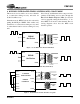
Table Of Contents
- Features
- Description
- 1. Pin Out - 144-Pin LQFP Package
- 2. Pin Out - 160-Ball FBGA Package
- 3. Pin Descriptions
- 4. operation
- 5. Power-up
- 6. Master Clock
- 7. G.772 Monitoring
- 8. Building Integrated Timing Systems (BITS) Clock Mode
- 9. Transmitter
- 10. Receiver
- 11. Jitter Attenuator
- 12. Operational Summary
- 13. Host Mode
- 14. Register Descriptions
- 14.1 Revision/IDcode Register (00h)
- 14.2 Analog Loopback Register (01h)
- 14.3 Remote Loopback Register (02h)
- 14.4 TAOS Enable Register (03h)
- 14.5 LOS Status Register (04h)
- 14.6 DFM Status Register (05h)
- 14.7 LOS Interrupt Enable Register (06h)
- 14.8 DFM Interrupt Enable Register (07h)
- 14.9 LOS Interrupt Status Register (08h)
- 14.10 DFM Interrupt Status Register (09h)
- 14.11 Software Reset Register (0Ah)
- 14.12 Performance Monitor Register (0Bh)
- 14.13 Digital Loopback Reset Register (0Ch)
- 14.14 LOS/AIS Mode Enable Register (0Dh)
- 14.15 Automatic TAOS Register (0Eh)
- 14.16 Global Control Register (0Fh)
- 14.17 Line Length Channel ID Register (10h)
- 14.18 Line Length Data Register (11h)
- 14.19 Output Disable Register (12h)
- 14.20 AIS Status Register (13h)
- 14.21 AIS Interrupt Enable Register (14h)
- 14.22 AIS Interrupt Status Register (15h)
- 14.23 AWG Broadcast Register (16h)
- 14.24 AWG Phase Address Register (17h)
- 14.25 AWG Phase Data Register (18h)
- 14.26 AWG Enable Register (19h)
- 14.27 Reserved Register (1Ah)
- 14.28 Reserved Register (1Bh)
- 14.29 Reserved Register (1Ch)
- 14.30 Reserved Register (1Dh)
- 14.31 Bits Clock Enable Register (1Eh)
- 14.32 Reserved Register (1Fh)
- 14.33 Status Registers
- 15. Arbitrary Waveform Generator
- 16. JTAG Support
- 17. Boundary Scan Register (BSR)
- 18. Applications
- 19. Characteristics and specifications
- 19.1 Absolute Maximum Ratings
- 19.2 Recommended Operating Conditions
- 19.3 Digital Characteristics
- 19.4 Transmitter Analog Characteristics
- 19.5 Receiver Analog Characteristics
- 19.6 Jitter Attenuator Characteristics
- 19.7 Master Clock Switching Characteristics
- 19.8 Transmit Switching Characteristics
- 19.9 Receive Switching Characteristics
- 19.10 Switching Characteristics - Serial Port
- 19.11 Switching Characteristics - Parallel Port (Multiplexed Mode)
- 19.12 Switching Characteristics- Parallel Port (Non-Multiplexed Mode)
- 19.13 Switching Characteristics - JTAG
- 20. Compliant Recommendations and specifications
- 21. 160-Ball FBGA package dimensions
- 22. 144-Pin LQFP Package dimensions
CS61880
24 DS450PP3
9. TRANSMITTER
The CS61880 contains eight identical transmitters
that each use a low power matched impedance driv-
er to eliminate the need for external load matching
resistors, while providing superior return loss. As a
result, the TTIP/TRING outputs can be connected
directly to the transformer allowing one hardware
circuit for E1 120 Ω, and E1 75 Ω applications.
Digital transmit data and clock are input into the
CS61880 through the TPOS/TDATA, TNEG and
TCLK input pins. These pins accept data in one of
three formats: unipolar, bipolar, or RZ. In either
unipolar or bipolar mode, the CS61880 internally
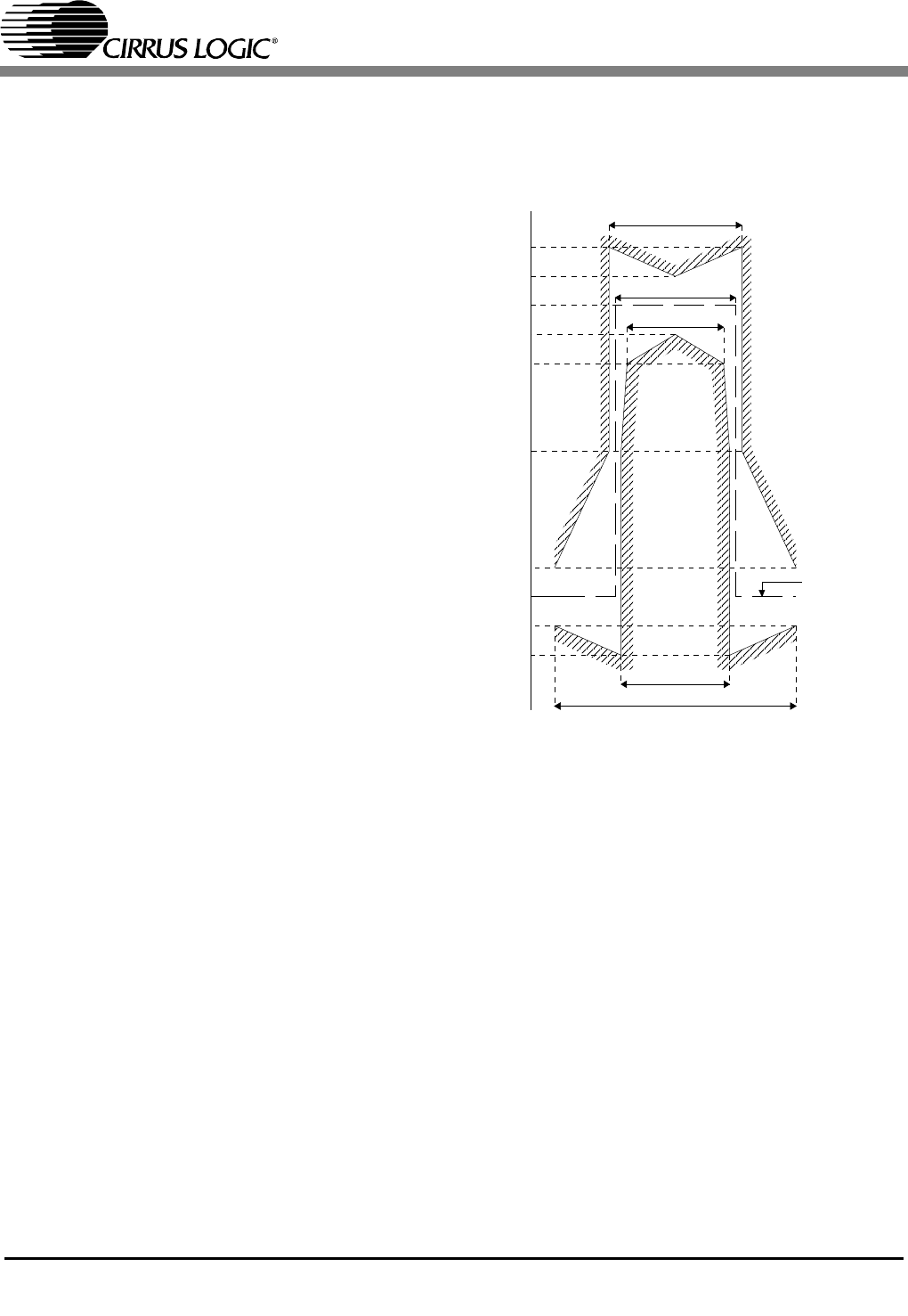
generates a pulse shape compliant to the G.703
mask for E1 (Refer to Figure 6). The pulse shaping
applied to the transmit data can be selected in hard-
ware mode or in host mode.
In hardware mode, the line impedance (75 Ω or
120 Ω) and which prestored pulse shape to transmit
(75 Ω or 120 Ω) is selected via the CBLSEL pin for
all eight transmitters.
In host mode, each channel is configured indepen-
dently by writing to the Line Length Channel ID
Register (10h) (See Section 14.17 on page 38),
then writing the desired line length settings to the
LEN[3:0] bits in the Line Length Data Register
(11h) (See Section 14.18 on page 38). The LEN
bits select the pulse shape and line impedance of
the addressed channel. In host mode, the CBLSEL
pin is not used.
NOTE: If one channel is configured for E1 75 Ω mode,
another channel can be configured for E1
120 Ω mode at the same time. This operation is
only allowed in host mode.
The CS61880 also allows the user to customize the
transmit pulse shapes to compensate for non-stan-
dard cables, transformers, or protection circuitry.
For further information on the AWG Refer to Ar-
bitrary Waveform Generator (See Section 15 on
page 42).
For more information on the host mode registers re-
fer to Register Descriptions (See Section 14 on
page 35).
9.1 Bipolar Mode
Bipolar mode provides transparent operation for
applications in which the line coding function is
performed by an external framing device. In this
mode, the falling edge of TCLK samples NRZ data
on TPOS/TNEG for transmission on TTIP/TRING.
9.2 Unipolar Mode
In unipolar mode, the CS61880 is configured such
that transmit data is encoded using HDB3, or AMI
line codes. This mode is activated by holding
269 ns
244 ns
194 ns
219 ns
488 ns
Nominal Puls
e
0
10
50
80
90
100
110
120
-10
-20
P
ercent of
n
ominal peak
v
oltage
Figure 6. Pulse Mask at E1 Interface