
User Manual
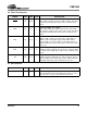
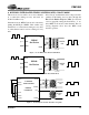
Table Of Contents
- Features
- Description
- 1. Pin Out - 144-Pin LQFP Package
- 2. Pin Out - 160-Ball FBGA Package
- 3. Pin Descriptions
- 4. operation
- 5. Power-up
- 6. Master Clock
- 7. G.772 Monitoring
- 8. Building Integrated Timing Systems (BITS) Clock Mode
- 9. Transmitter
- 10. Receiver
- 11. Jitter Attenuator
- 12. Operational Summary
- 13. Host Mode
- 14. Register Descriptions
- 14.1 Revision/IDcode Register (00h)
- 14.2 Analog Loopback Register (01h)
- 14.3 Remote Loopback Register (02h)
- 14.4 TAOS Enable Register (03h)
- 14.5 LOS Status Register (04h)
- 14.6 DFM Status Register (05h)
- 14.7 LOS Interrupt Enable Register (06h)
- 14.8 DFM Interrupt Enable Register (07h)
- 14.9 LOS Interrupt Status Register (08h)
- 14.10 DFM Interrupt Status Register (09h)
- 14.11 Software Reset Register (0Ah)
- 14.12 Performance Monitor Register (0Bh)
- 14.13 Digital Loopback Reset Register (0Ch)
- 14.14 LOS/AIS Mode Enable Register (0Dh)
- 14.15 Automatic TAOS Register (0Eh)
- 14.16 Global Control Register (0Fh)
- 14.17 Line Length Channel ID Register (10h)
- 14.18 Line Length Data Register (11h)
- 14.19 Output Disable Register (12h)
- 14.20 AIS Status Register (13h)
- 14.21 AIS Interrupt Enable Register (14h)
- 14.22 AIS Interrupt Status Register (15h)
- 14.23 AWG Broadcast Register (16h)
- 14.24 AWG Phase Address Register (17h)
- 14.25 AWG Phase Data Register (18h)
- 14.26 AWG Enable Register (19h)
- 14.27 Reserved Register (1Ah)
- 14.28 Reserved Register (1Bh)
- 14.29 Reserved Register (1Ch)
- 14.30 Reserved Register (1Dh)
- 14.31 Bits Clock Enable Register (1Eh)
- 14.32 Reserved Register (1Fh)
- 14.33 Status Registers
- 15. Arbitrary Waveform Generator
- 16. JTAG Support
- 17. Boundary Scan Register (BSR)
- 18. Applications
- 19. Characteristics and specifications
- 19.1 Absolute Maximum Ratings
- 19.2 Recommended Operating Conditions
- 19.3 Digital Characteristics
- 19.4 Transmitter Analog Characteristics
- 19.5 Receiver Analog Characteristics
- 19.6 Jitter Attenuator Characteristics
- 19.7 Master Clock Switching Characteristics
- 19.8 Transmit Switching Characteristics
- 19.9 Receive Switching Characteristics
- 19.10 Switching Characteristics - Serial Port
- 19.11 Switching Characteristics - Parallel Port (Multiplexed Mode)
- 19.12 Switching Characteristics- Parallel Port (Non-Multiplexed Mode)
- 19.13 Switching Characteristics - JTAG
- 20. Compliant Recommendations and specifications
- 21. 160-Ball FBGA package dimensions
- 22. 144-Pin LQFP Package dimensions
CS61880
22 DS450PP3
4. OPERATION
The CS61880 is a full featured line interface unit
for up to eight E1 75 Ω or E1 120 Ω lines. The de-
vice provides an interface to twisted pair or co-ax-
ial media. A matched impedance technique is
employed that reduces power and eliminates the
need for matching resistors. As a result, the device
can interface directly to the line through a trans-
former without the need for matching resistors on
the transmit side. The receive side uses the same re-
sistor values for all E1 settings.
5. POWER-UP
On power-up, the device is held in a static state un-
til the power supply achieves approximately 70%
of the power supply voltage. Once the power sup-
ply threshold is passed, the analog circuitry is cali-
brated, the control registers are reset to their default
settings, and the various internal state machines are
reset. The reset/calibration process completes in
about 30 ms.
6. MASTER CLOCK
The CS61880 requires a 2.048 MHz reference
clock with a minimum accuracy of ±100 ppm. This
clock may be supplied from internal system timing
or a CMOS crystal oscillator and input to the
MCLK pin.
The receiver uses MCLK as a reference for clock
recovery, jitter attenuation, and the generation of
RCLK during LOS. The transmitter uses MCLK as
the transmit timing reference during a blue alarm
transmit all ones condition. In addition, MCLK
provides the reference timing for wait state genera-
tion.
In systems with a jittered transmit clock, MCLK
should not be tied to the transmit clock, a separate
crystal oscillator should drive the reference clock
input. Any jitter present on the reference clock will
not be filtered by the jitter attenuator and can cause
the CS61880 to operate incorrectly.
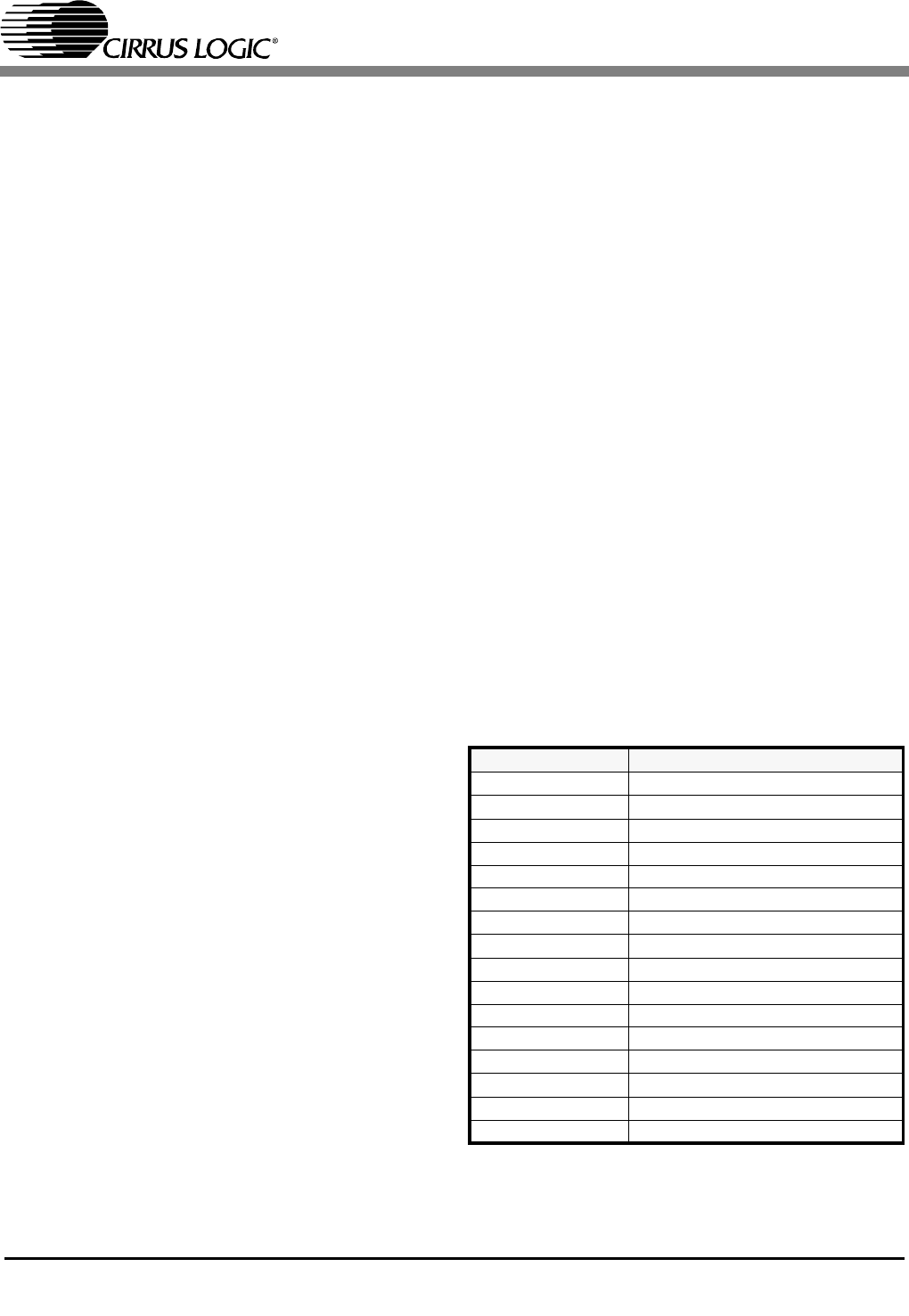
7. G.772 MONITORING
The receive path of channel zero of the CS61880
can be used to monitor the receive or transmit paths
of any of the other channels. The signal to be mon-
itored is multiplexed to channel zero through the
G.772 Multiplexer. The multiplexer and channel
zero then form a G.772 compliant digital Protected
Monitoring Point (PMP). When the PMP is connect-
ed to the channel, the attenuation in the signal path is
negligible across the signal band. The signal can be
observed using RPOS, RNEG, and RCLK of chan-
nel zero or by putting channel zero in remote loop-
back, the signal can be observed on TTIP and
TRING of channel zero.
The G.772 monitoring function is available during
both host mode and hardware mode operation. In
host modes, individual channels are selected for
monitoring via the Performance Monitor Regis-
ter (0Bh) (See Section 14.12 on page 36)). In hard-
ware mode, individual channels are selected
through the A3:A0 pins (Refer to Table 6 below for
address settings).
NOTE: In hardware mode the A4 pin must be tied low
at all times.
Table 6. G.772 Address Selection
Address [A3:A0] Channel Selection
0000 Monitoring Disabled
0001 Receiver Channel # 1
0010 Receiver Channel # 2
0011 Receiver Channel # 3
0100 Receiver Channel # 4
0101 Receiver Channel # 5
0110 Receiver Channel # 6
0111 Receiver Channel # 7
1000 Monitoring Disabled
1001 Transmitter Channel # 1
1010 Transmitter Channel # 2
1011 Transmitter Channel # 3
1100 Transmitter Channel # 4
1101 Transmitter Channel # 5
1110 Transmitter Channel # 6
1111 Transmitter Channel # 7