
User Manual
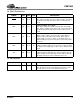
Table Of Contents
- Features
- Description
- 1. Pin Out - 144-Pin LQFP Package
- 2. Pin Out - 160-Ball FBGA Package
- 3. Pin Descriptions
- 4. operation
- 5. Power-up
- 6. Master Clock
- 7. G.772 Monitoring
- 8. Building Integrated Timing Systems (BITS) Clock Mode
- 9. Transmitter
- 10. Receiver
- 11. Jitter Attenuator
- 12. Operational Summary
- 13. Host Mode
- 14. Register Descriptions
- 14.1 Revision/IDcode Register (00h)
- 14.2 Analog Loopback Register (01h)
- 14.3 Remote Loopback Register (02h)
- 14.4 TAOS Enable Register (03h)
- 14.5 LOS Status Register (04h)
- 14.6 DFM Status Register (05h)
- 14.7 LOS Interrupt Enable Register (06h)
- 14.8 DFM Interrupt Enable Register (07h)
- 14.9 LOS Interrupt Status Register (08h)
- 14.10 DFM Interrupt Status Register (09h)
- 14.11 Software Reset Register (0Ah)
- 14.12 Performance Monitor Register (0Bh)
- 14.13 Digital Loopback Reset Register (0Ch)
- 14.14 LOS/AIS Mode Enable Register (0Dh)
- 14.15 Automatic TAOS Register (0Eh)
- 14.16 Global Control Register (0Fh)
- 14.17 Line Length Channel ID Register (10h)
- 14.18 Line Length Data Register (11h)
- 14.19 Output Disable Register (12h)
- 14.20 AIS Status Register (13h)
- 14.21 AIS Interrupt Enable Register (14h)
- 14.22 AIS Interrupt Status Register (15h)
- 14.23 AWG Broadcast Register (16h)
- 14.24 AWG Phase Address Register (17h)
- 14.25 AWG Phase Data Register (18h)
- 14.26 AWG Enable Register (19h)
- 14.27 Reserved Register (1Ah)
- 14.28 Reserved Register (1Bh)
- 14.29 Reserved Register (1Ch)
- 14.30 Reserved Register (1Dh)
- 14.31 Bits Clock Enable Register (1Eh)
- 14.32 Reserved Register (1Fh)
- 14.33 Status Registers
- 15. Arbitrary Waveform Generator
- 16. JTAG Support
- 17. Boundary Scan Register (BSR)
- 18. Applications
- 19. Characteristics and specifications
- 19.1 Absolute Maximum Ratings
- 19.2 Recommended Operating Conditions
- 19.3 Digital Characteristics
- 19.4 Transmitter Analog Characteristics
- 19.5 Receiver Analog Characteristics
- 19.6 Jitter Attenuator Characteristics
- 19.7 Master Clock Switching Characteristics
- 19.8 Transmit Switching Characteristics
- 19.9 Receive Switching Characteristics
- 19.10 Switching Characteristics - Serial Port
- 19.11 Switching Characteristics - Parallel Port (Multiplexed Mode)
- 19.12 Switching Characteristics- Parallel Port (Non-Multiplexed Mode)
- 19.13 Switching Characteristics - JTAG
- 20. Compliant Recommendations and specifications
- 21. 160-Ball FBGA package dimensions
- 22. 144-Pin LQFP Package dimensions
CS61880
DS450PP3 21
3.8 JTAG Test Interface
3.9 Miscellaneous
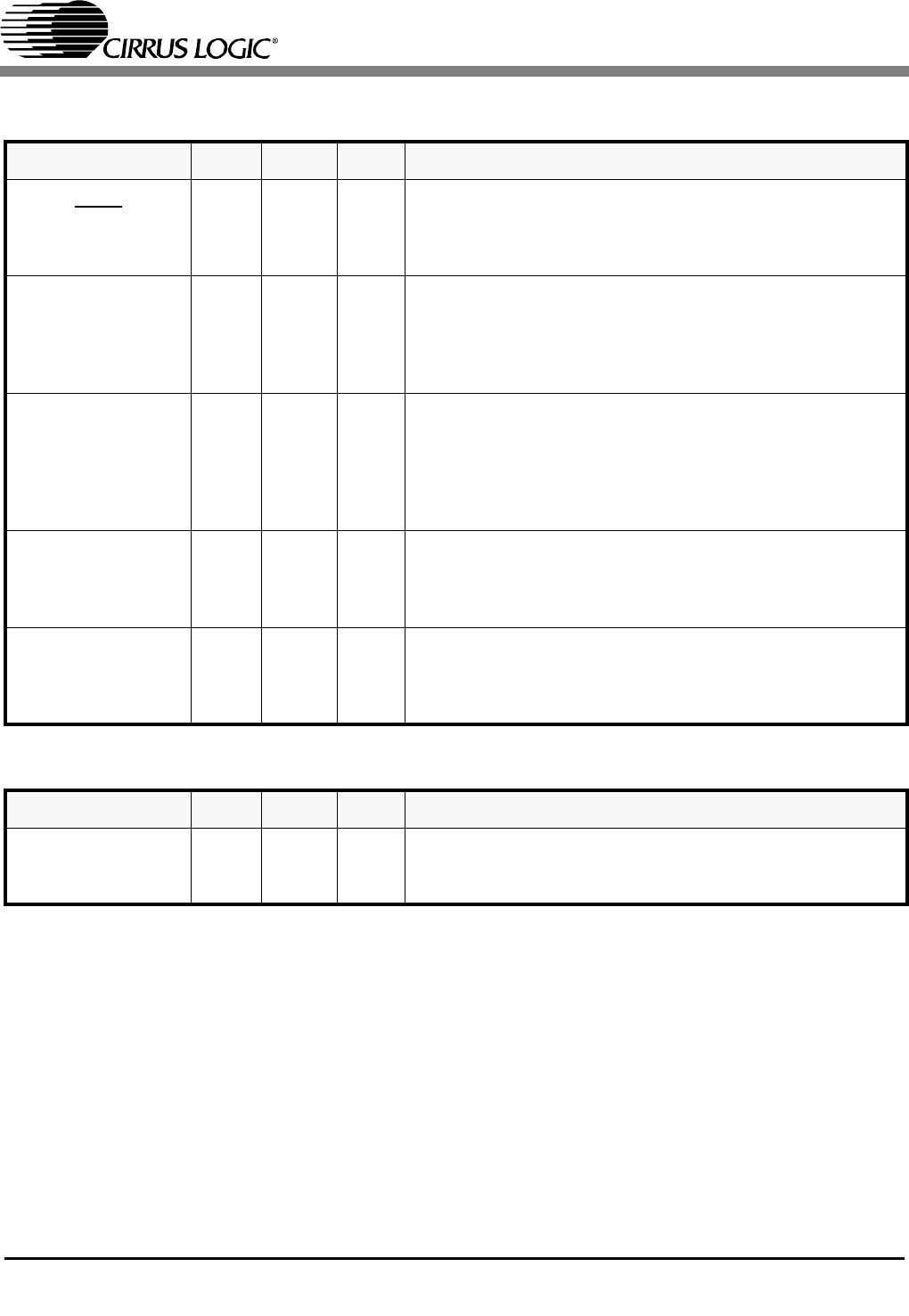
SYMBOL LQFP FBGA TYPE DESCRIPTION
TRST
95 G12 I
JTAG Reset
This active Low input resets the JTAG controller. This input
is pulled up internally and may be left as a NC when not
used.
TMS 96 F11 I
JTAG Test Mode Select Input
This input enables the JTAG serial port when active High.
This input is sampled on the rising edge of TCK. This input
is pulled up internally and may be left as a NC when not
used.
TCK 97 F14 I
JTAG Test Clock
Data on TDI is valid on the rising edge of TCK. Data on
TDO is valid on the falling edge of TCK. When TCK is
stopped high or low, the contents of all JTAG registers re-
main unchanged. Tie pin low through a 10 kΩ resistor when
not used.
TDO 98 F13 O
JTAG Test Data Output
JTAG test data is shifted out of the device on this pin. Data
is output on the falling edge of TCK. Leave as NC when not
used.
TDI 99 F12 I
JTAG Test Data Input
JTAG test data is shifted into the device using this pin. The
pin is sampled on the rising edge of TCK. TDI is pulled up
internally and may be left as a NC when not used.
SYMBOL LQFP FBGA TYPE DESCRIPTION
REF 94 H13 I Reference Input
This pin must be tied to ground through 13.3 kΩ 1% resis-
tor. This pin is used to set the internal current level.