
User Manual
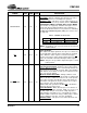
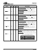
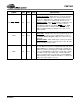
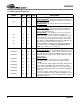
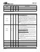
Table Of Contents
- Features
- Description
- 1. Pin Out - 144-Pin LQFP Package
- 2. Pin Out - 160-Ball FBGA Package
- 3. Pin Descriptions
- 4. operation
- 5. Power-up
- 6. Master Clock
- 7. G.772 Monitoring
- 8. Building Integrated Timing Systems (BITS) Clock Mode
- 9. Transmitter
- 10. Receiver
- 11. Jitter Attenuator
- 12. Operational Summary
- 13. Host Mode
- 14. Register Descriptions
- 14.1 Revision/IDcode Register (00h)
- 14.2 Analog Loopback Register (01h)
- 14.3 Remote Loopback Register (02h)
- 14.4 TAOS Enable Register (03h)
- 14.5 LOS Status Register (04h)
- 14.6 DFM Status Register (05h)
- 14.7 LOS Interrupt Enable Register (06h)
- 14.8 DFM Interrupt Enable Register (07h)
- 14.9 LOS Interrupt Status Register (08h)
- 14.10 DFM Interrupt Status Register (09h)
- 14.11 Software Reset Register (0Ah)
- 14.12 Performance Monitor Register (0Bh)
- 14.13 Digital Loopback Reset Register (0Ch)
- 14.14 LOS/AIS Mode Enable Register (0Dh)
- 14.15 Automatic TAOS Register (0Eh)
- 14.16 Global Control Register (0Fh)
- 14.17 Line Length Channel ID Register (10h)
- 14.18 Line Length Data Register (11h)
- 14.19 Output Disable Register (12h)
- 14.20 AIS Status Register (13h)
- 14.21 AIS Interrupt Enable Register (14h)
- 14.22 AIS Interrupt Status Register (15h)
- 14.23 AWG Broadcast Register (16h)
- 14.24 AWG Phase Address Register (17h)
- 14.25 AWG Phase Data Register (18h)
- 14.26 AWG Enable Register (19h)
- 14.27 Reserved Register (1Ah)
- 14.28 Reserved Register (1Bh)
- 14.29 Reserved Register (1Ch)
- 14.30 Reserved Register (1Dh)
- 14.31 Bits Clock Enable Register (1Eh)
- 14.32 Reserved Register (1Fh)
- 14.33 Status Registers
- 15. Arbitrary Waveform Generator
- 16. JTAG Support
- 17. Boundary Scan Register (BSR)
- 18. Applications
- 19. Characteristics and specifications
- 19.1 Absolute Maximum Ratings
- 19.2 Recommended Operating Conditions
- 19.3 Digital Characteristics
- 19.4 Transmitter Analog Characteristics
- 19.5 Receiver Analog Characteristics
- 19.6 Jitter Attenuator Characteristics
- 19.7 Master Clock Switching Characteristics
- 19.8 Transmit Switching Characteristics
- 19.9 Receive Switching Characteristics
- 19.10 Switching Characteristics - Serial Port
- 19.11 Switching Characteristics - Parallel Port (Multiplexed Mode)
- 19.12 Switching Characteristics- Parallel Port (Non-Multiplexed Mode)
- 19.13 Switching Characteristics - JTAG
- 20. Compliant Recommendations and specifications
- 21. 160-Ball FBGA package dimensions
- 22. 144-Pin LQFP Package dimensions
CS61880
DS450PP3 19
3.7 Analog RX/TX Data I/O
RCLK7 143 A1 O Receive Clock Output Port 7
RPOS7/RDATA7 142 A2 O Receive Positive Pulse/ Receive Data Output Port 7
RNEG7/BPV7 141 A3 O Receive Negative Pulse/Bipolar Violation Output Port 7
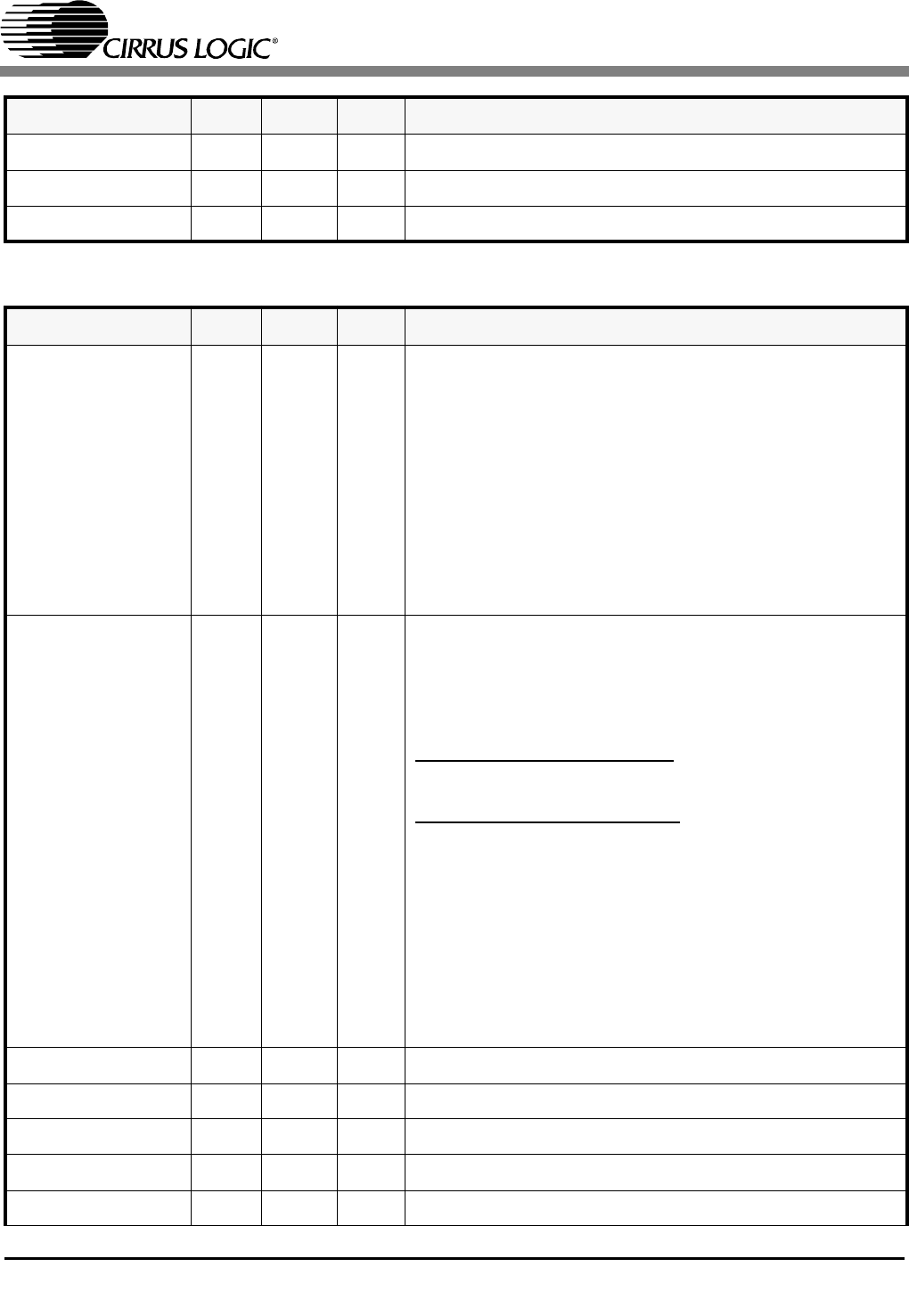
SYMBOL LQFP FBGA TYPE DESCRIPTION
SYMBOL LQFP FBGA TYPE DESCRIPTION
TTIP0
TRING0
45
46
N5
P5
O
O
Transmit Tip Output Port 0
Transmit Ring Output Port 0
These pins are the differential outputs of the transmit driver.
The driver internally matches impedances for E1 75 Ω or
E1 120 Ω lines requiring only a 1:1.15 transformer. The
CBLSEL pin is used to select the appropriate line matching
impedance only in “Hardware” mode. In host mode, the ap-
propriate line matching impedance is selected by the Line
Length Data Register (11h) (See Section 14.18 on
page 38).
NOTE: TTIP and TRING are forced to a high impedance state
when the TCLK or the TXOE pin is forced “Low”.
RTIP0
RRING0
48
49
P7
N7
I
I
Receive Tip Input Port 0
Receive Ring Input Port 0
These pins are the differential line inputs to the receiver.
The receiver uses either Internal Line Impedance or Exter-
nal Line Impedance modes to match the line impedances
for E1 75Ω or E1 120Ω modes.
Internal Line Impedance Mode
- The receiver uses the
same external resistors to match the line impedance (Refer
to Figure 16 on page 50).
External Line Impedance Mode
- The receiver uses differ-
ent external resistors to match the line impedance (Refer to
Figure 17 on page 51).
- In host mode, the appropriate line impedance is selected
by the Line Length Data Register (11h) (See Section
14.18 on page 38).
- In hardware mode, the CBLSEL pin selects the appropri-
ate line impedance. (Refer to Table 4 on page 15 for proper
line impedance settings).
NOTE: Data and clock recovered from the signal input on
these pins are output via RCLK, RPOS, and RNEG.
TTIP1 52 L5 O Transmit Tip Output Port 1
TRING1 51 M5 O Transmit Ring Output Port 1
RTIP1 55 M7 I Receive Tip Input Port 1
RRING1 54 L7 I Receive Ring Input Port 1
TTIP2 57 L10 O Transmit Tip Output Port 2